ZHCSD49 December 2014 TPS62160-Q1
PRODUCTION DATA.
- 1 特性
- 2 应用
- 3 说明
- 4 简化电路原理图
- 5 修订历史记录
- 6 Pin Configuration and Functions
- 7 Specifications
- 8 Detailed Description
- 9 Application and Implementation
- 10Power Supply Recommendations
- 11Layout
- 12器件和文档支持
- 13机械封装和可订购信息
7 Specifications
7.1 Absolute Maximum Ratings
over operating junction temperature range (unless otherwise noted)(1)| MIN | MAX | UNIT | ||
|---|---|---|---|---|
| Pin voltage range(2) | VIN | –0.3 | 20 | V |
| EN, SW | –0.3 | VIN+0.3 | V | |
| FB, PG, VOS | –0.3 | 7 | V | |
| Power Good sink current | PG | 10 | mA | |
| Operating junction temperature range, TJ | –40 | 125 | °C | |
| Storage temperature range, Tstg | –65 | 150 | °C | |
(1) Stresses beyond those listed under absolute maximum ratings may cause permanent damage to the device. These are stress ratings only, and functional operation of the device at these or any other conditions beyond those indicated under recommended operating conditions is not implied. Exposure to absolute-maximum-rated conditions for extended periods my affect device reliability.
(2) All voltages are with respect to network ground terminal.
7.2 ESD Ratings
| VALUE | UNIT | ||||
|---|---|---|---|---|---|
| V(ESD) | Electrostatic discharge | Human body model (HBM), per AEC Q100-002(1) | ±2000 | V | |
| Charged device model (CDM), per AEC Q100-011 | ±500 | ||||
(1) AEC Q100-002 indicates HBM stressing is done in accordance with the ANSI/ESDA/JEDEC JS-001 specification.
7.3 Recommended Operating Conditions
over operating junction temperature range (unless otherwise noted)| MIN | TYP | MAX | UNIT | ||
|---|---|---|---|---|---|
| VIN | Supply voltage | 3 | 17 | V | |
| VOUT | Output voltage range | 0.9 | 6 | V | |
| TJ | Operating junction temperature | –40 | 125 | °C | |
7.4 Thermal Information
| THERMAL METRIC(1) | TPS62160-Q1 | UNIT | ||
|---|---|---|---|---|
| DSG (8 PINS) | DGK (8 PINS) | |||
| RθJA | Junction-to-ambient thermal resistance | 61.8 | 184.3 | °C/W |
| RθJC(top) | Junction-to-case (top) thermal resistance | 61.3 | 74.6 | |
| RθJB | Junction-to-board thermal resistance | 15.5 | 105.8 | |
| ψJT | Junction-to-top characterization parameter | 0.4 | 13.3 | |
| ψJB | Junction-to-board characterization parameter | 15.4 | 104.2 | |
| RθJC(bot) | Junction-to-case (bottom) thermal resistance | 8.6 | - | |
(1) For more information about traditional and new thermal metrics, see the IC Package Thermal Metrics application report, SPRA953.
7.5 Electrical Characteristics
Over junction temperature range (TJ = –40°C to +125°C), typical values at VIN = 12 V and TJ = 25°C (unless otherwise noted)| PARAMETER | TEST CONDITIONS | MIN | TYP | MAX | UNIT | ||
|---|---|---|---|---|---|---|---|
| SUPPLY | |||||||
| VIN | Input voltage range(1) | 3 | 17 | V | |||
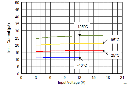
| IQ | Operating quiescent current | EN = High, IOUT = 0 mA, Device not switching | 17 | 30 | µA | ||
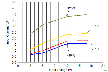
| ISD | Shutdown current(2) | EN = Low | 1.8 | 25 | µA | ||
| VUVLO | Undervoltage lockout threshold | Falling input voltage | 2.6 | 2.7 | 2.82 | V | |
| Hysteresis | 180 | mV | |||||
| TSD | Thermal shutdown temperature | 160 | °C | ||||
| Thermal shutdown hysteresis | 20 | ||||||
| CONTROL (EN, PG) | |||||||
| VEN_H | High level input threshold voltage (EN) | 0.9 | V | ||||
| VEN_L | Low level input threshold voltage (EN) | 0.3 | V | ||||
| ILKG_EN | Input leakage current (EN) | EN = VIN or GND | 0.01 | 1 | µA | ||
| VTH_PG | Power Good threshold voltage | Rising (%VOUT) | 92% | 95% | 98% | ||
| Falling (%VOUT) | 87% | 90% | 93% | ||||
| VOL_PG | Power Good output low | IPG = –2 mA | 0.07 | 0.3 | V | ||
| ILKG_PG | Input leakage current (PG) | VPG = 1.8 V | 1 | 400 | nA | ||
| POWER SWITCH | |||||||
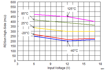
| RDS(ON) | High-side MOSFET ON-resistance | VIN ≥ 6 V | 300 | 600 | mΩ | ||
| VIN = 3 V | 430 | ||||||
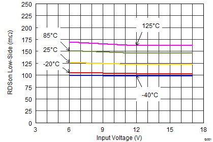
| Low-side MOSFET ON-resistance | VIN ≥ 6 V | 120 | 200 | mΩ | |||
| VIN = 3 V | 165 | ||||||
| ILIMF | High-side MOSFET forward current limit(3) | VIN = 12 V, TA = 25°C | 1.45 | 1.95 | 2.45 | A | |
| OUTPUT | |||||||
| VREF | Internal reference voltage | 0.8 | V | ||||
| ILKG_FB | Pin leakage current (FB) | VFB = 1.2 V | 5 | 400 | nA | ||
| VOUT | Output voltage range | VIN ≥ VOUT | 0.9 | 6.0 | V | ||
| Feedback voltage accuracy | PWM Mode operation, VIN ≥ VOUT + 1 V | –3% | 3% | ||||
| Power Save Mode operation, COUT = 2x22 µF(4) | –3% | 4% | |||||
| DC output voltage load regulation(5) | VIN = 12 V, VOUT = 3.3 V, PWM Mode operation | 0.05 | % / A | ||||
| DC output voltage line regulation (5) | 3 V ≤ VIN ≤ 17 V, VOUT = 3.3 V, IOUT = 0.5 A, PWM Mode operation | 0.02 | % / V | ||||
(1) The device is still functional down to Under Voltage Lockout (see parameter VUVLO).
(2) Current into VIN pin.
(3) This is the static current limit. It can be temporarily higher in applications due to internal propagation delay (see Current Limit and Short Circuit Protection section).
(4) The accuracy in Power Save Mode can be improved by increasing the COUT value, reducing the output voltage ripple.
7.6 Typical Characteristics
At VIN = 12 V, VOUT = 3.3 V and TJ = 25°C (unless otherwise noted)