ZHCSD49 December 2014 TPS62160-Q1
PRODUCTION DATA.
- 1 特性
- 2 应用
- 3 说明
- 4 简化电路原理图
- 5 修订历史记录
- 6 Pin Configuration and Functions
- 7 Specifications
- 8 Detailed Description
- 9 Application and Implementation
- 10Power Supply Recommendations
- 11Layout
- 12器件和文档支持
- 13机械封装和可订购信息
9 Application and Implementation
9.1 Application Information
The TPS62160-Q1 is a synchronous switched mode step-down converter, able to convert a 3 V to 17 V input voltage into a lower, 0.9 V to 6 V, output voltage, providing up to 1-A load current. The following section gives guidance on the external component selection to operate the device within the recommended operating conditions.
9.2 Typical TPS62160-Q1 Application
 Figure 5. 3.3-V / 1-A Power Supply
9.2.1 Design Requirements
The step-down converter design can be adapted to different output voltage and load current needs by choosing external components appropriate. The following design procedure is adequate for whole VIN, VOUT, and load current range of TPS62160-Q1. Using Table 2, the design procedure needs minimum effort.
Table 1. Components Used for Application Characteristics
| REFERENCE | DESCRIPTION | MANUFACTURER |
|---|---|---|
| IC | 17-V, 1-A step-down converter, WSON | TPS62160QDSG, Texas Instruments |
| L1 | 2.2-µH, 1.4-A, 3 x 2.8 x 1.2 mm | VLF3012ST-2R2M1R4, TDK |
| CIN | 10-µF, 25-V, ceramic | Standard |
| COUT | 22-µF, 6.3-V, ceramic | Standard |
| R1 | Depending on Vout | |
| R2 | Depending on Vout | |
| R3 | 100-kΩ, chip, 0603, 1/16-W, 1% | Standard |
9.2.2 Detailed Design Procedure
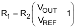
9.2.2.1 Programming the Output Voltage
The TPS62160-Q1 can be programmed for output voltages from 0.9 V to 6 V by using a resistive divider from VOUT to FB to AGND. The voltage at the FB pin is regulated to 800 mV. The value of the output voltage is set by the selection of the resistive divider from Equation 6. It is recommended to choose resistor values which allow a cross current of at least 2 uA, meaning the value of R2 should not exceed 400 kΩ. Lower resistor values are recommended for highest accuracy and most robust design. For applications requiring lowest current consumption, the use of fixed output voltage versions is recommended.
In case the FB pin gets opened, the device clamps the output voltage at the VOS pin to about 7.4 V.
9.2.2.2 External Component Selection
The external components have to fulfill the needs of the application, but also the stability criteria of the devices control loop. The TPS62160-Q1 is optimized to work within a range of external components. The LC output filters inductance and capacitance have to be considered together, creating a double pole, responsible for the corner frequency of the converter (see Output Filter And Loop Stability section). Table 2 can be used to simplify the output filter component selection.
Table 2. Recommended LC Output Filter Combinations(1)
| 4.7µF | 10µF | 22µF | 47µF | 100µF | 200µF | 400µF | |
|---|---|---|---|---|---|---|---|
| 1µH | |||||||
| 2.2µH | √ | √(2) | √ | √ | √ | ||
| 3.3µH | √ | √ | √ | √ | |||
| 4.7µH |
More detailed information on further LC combinations can be found in SLVA463.
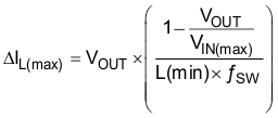
9.2.2.2.1 Inductor Selection
The inductor selection is affected by several effects like inductor ripple current, output ripple voltage, PWM-to-PSM transition point and efficiency. In addition, the inductor selected has to be rated for appropriate saturation current and DC resistance (DCR). Equation 7 and Equation 8 calculate the maximum inductor current under static load conditions.
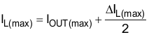
where
IL(max) is the maximum inductor current,
ΔIL is the Peak-to-Peak Inductor Ripple Current,
L(min) is the minimum effective inductor value and
fSW is the actual PWM Switching Frequency.
Calculating the maximum inductor current using the actual operating conditions gives the minimum saturation current of the inductor needed. A margin of about 20% is recommended to add. A larger inductor value is also useful to get lower ripple current, but increases the transient response time and size as well. The following inductors have been used with the TPS62160-Q1 and are recommended for use:
Table 3. List of Inductors
| TYPE | INDUCTANCE [µH] | CURRENT [A](1) | DIMENSIONS [L x B x H] mm | MANUFACTURER |
|---|---|---|---|---|
| VLF3012ST-2R2M1R4 | 2.2 µH, ±20% | 1.9 A | 3.0 x 2.8 x 1.2 | TDK |
| VLF302512MT-2R2M | 2.2 µH, ±20% | 1.9 A | 3.0 x 2.5 x 1.2 | TDK |
| VLS252012T-2R2M1R3 | 2.2 µH, ±20% | 1.3 A | 2.5 x 2.0 x 1.2 | TDK |
| XFL3012-222MEC | 2.2 µH, ±20% | 1.9 A | 3.0 x 3.0 x 1.2 | Coilcraft |
| XFL3012-332MEC | 3.3 µH, ±20% | 1.6 A | 3.0 x 3.0 x 1.2 | Coilcraft |
| LPS3015-332ML_ | 3.3 µH, ±20% | 1.4 A | 3.0 x 3.0 x 1.4 | Coilcraft |
| NR3015T-2R2M | 2.2 µH, ±20% | 1.5 A | 3.0 x 3.0 x 1.5 | Taiyo Yuden |
| 744025003 | 3.3 µH, ±20% | 1.5 A | 2.8 x 2.8 x 2.8 | Wuerth |
| PSI25201B-2R2MS | 2.2 µH, ±20% | 1.3 A | 2.0 x 2.5 x 1.2 | Cyntec |
The TPS62160-Q1 can be run with an inductor as low as 2.2 µH. However, for applications with low input voltages, 3.3 µH is recommended, to allow the full output current. The inductor value also determines the load current at which Power Save Mode is entered:
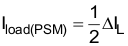
Using Equation 8, this current level can be adjusted by changing the inductor value.
9.2.2.2.2 Capacitor Selection
9.2.2.2.2.1 Output Capacitor
The recommended value for the output capacitor is 22 uF. The architecture of the TPS62160-Q1 allows the use of tiny ceramic output capacitors with low equivalent series resistance (ESR). These capacitors provide low output voltage ripple and are recommended. To keep its low resistance up to high frequencies and to get narrow capacitance variation with temperature, it's recommended to use X7R or X5R dielectric. Using a higher value can have some advantages like smaller voltage ripple and a tighter DC output accuracy in Power Save Mode (see SLVA463).
NOTE
In power save mode, the output voltage ripple depends on the output capacitance, its ESR and the peak inductor current. Using ceramic capacitors provides small ESR and low ripple.
9.2.2.2.2.2 Input Capacitor
For most applications, 10 µF is sufficient and is recommended, though a larger value reduces input current ripple further. The input capacitor buffers the input voltage for transient events and also decouples the converter from the supply. A low ESR multilayer ceramic capacitor is recommended for best filtering and should be placed between VIN and GND as close as possible to those pins.
NOTE
DC Bias effect: High capacitance ceramic capacitors have a DC Bias effect, which will have a strong influence on the final effective capacitance. Therefore the right capacitor value has to be chosen carefully. Package size and voltage rating in combination with dielectric material are responsible for differences between the rated capacitor value and the effective capacitance.
9.2.2.3 Output Filter And Loop Stability
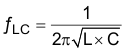
The TPS62160-Q1 is internally compensated to be stable with L-C filter combinations corresponding to a corner frequency to be calculated with Equation 10:
Proven nominal values for inductance and ceramic capacitance are given in Table 2 and are recommended for use. Different values may work, but care has to be taken on the loop stability which might be affected. More information including a detailed L-C stability matrix can be found in SLVA463.
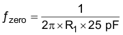
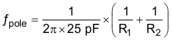
The TPS62160-Q1 includes an internal 25-pF feedforward capacitor, connected between the VOS and FB pins. This capacitor impacts the frequency behavior and sets a pole and zero in the control loop with the resistors of the feedback divider, per Equation 11 and Equation 12:
Though the TPS62160-Q1 is stable without the pole and zero being in a particular location, adjusting their location to the specific needs of the application can provide better performance in Power Save mode and/or improved transient response. An external feedforward capacitor can also be added. A more detailed discussion on the optimization for stability vs transient response can be found in SLVA289 and SLVA466.
If using ceramic capacitors, the DC bias effect has to be considered. The DC bias effect results in a drop in effective capacitance as the voltage across the capacitor increases (see NOTE in DC Bias effect section).
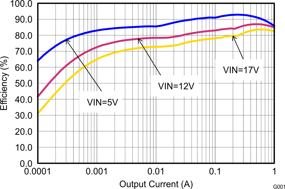
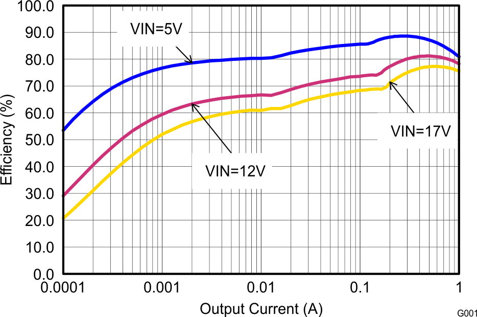
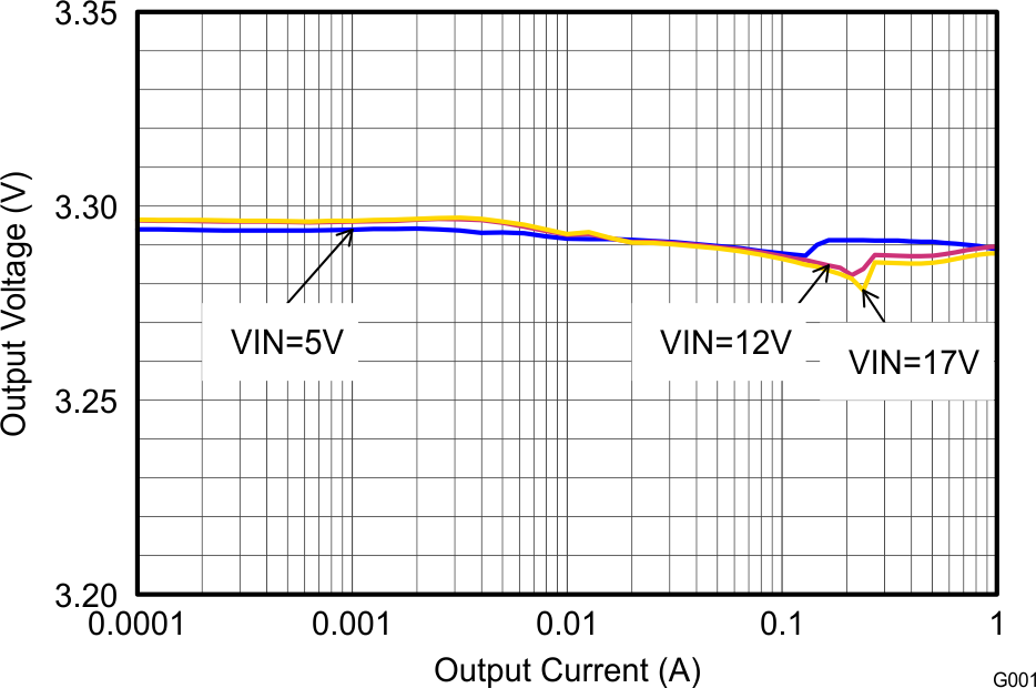
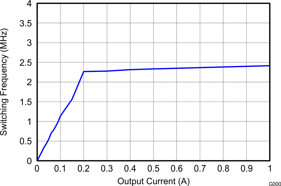
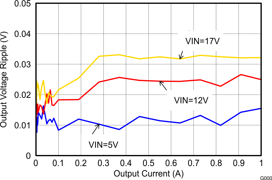
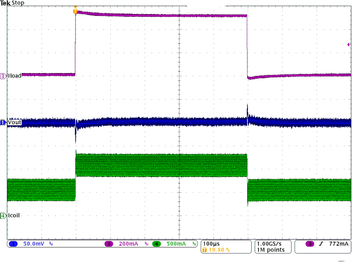
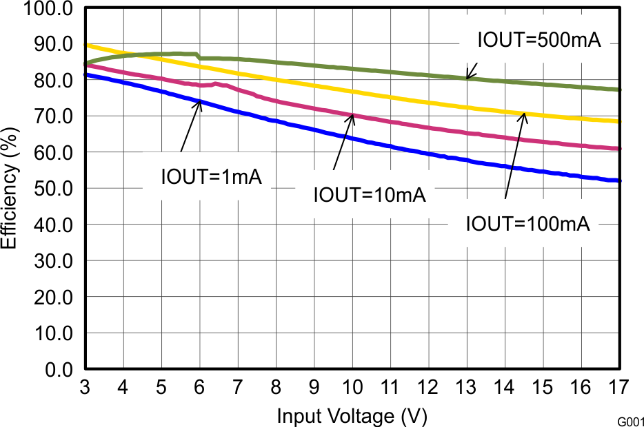
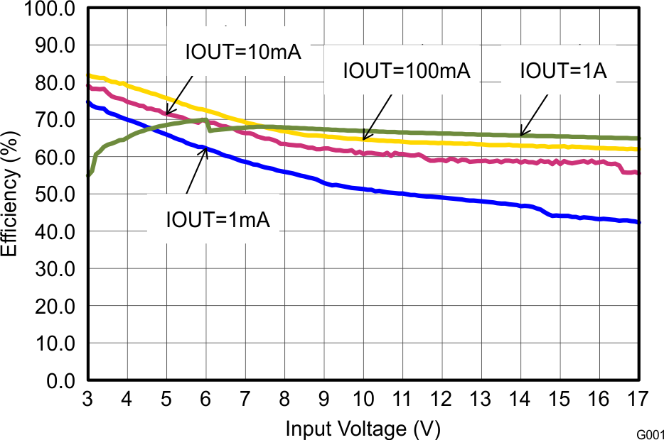
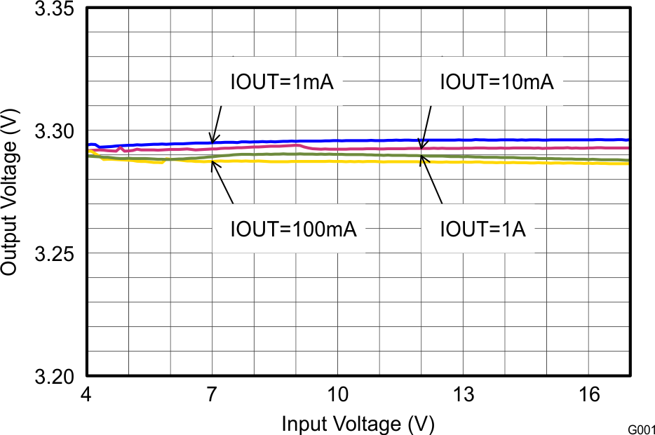
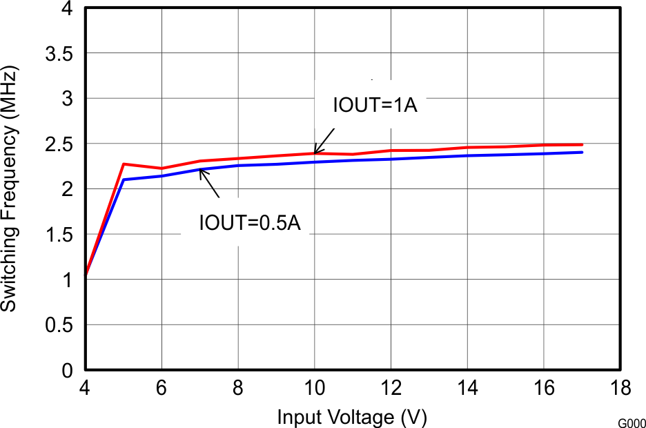
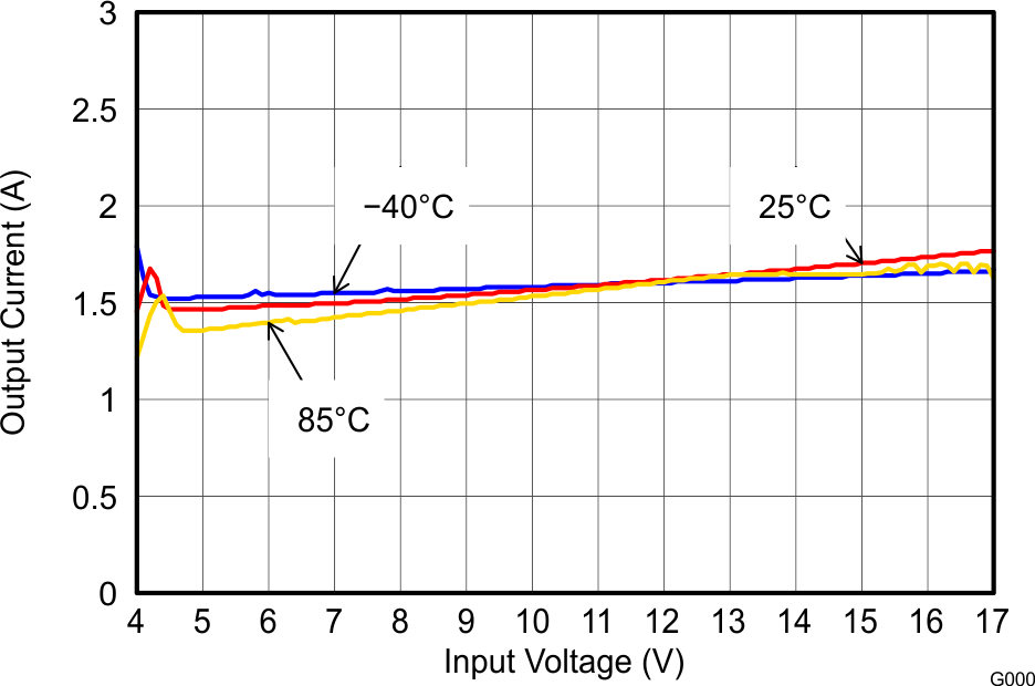
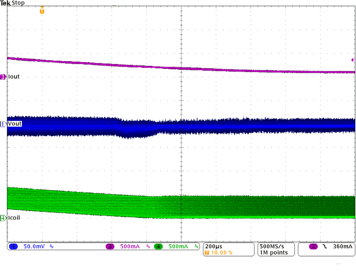
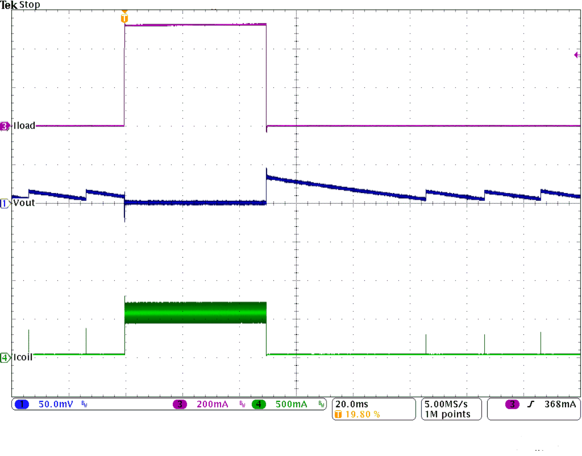
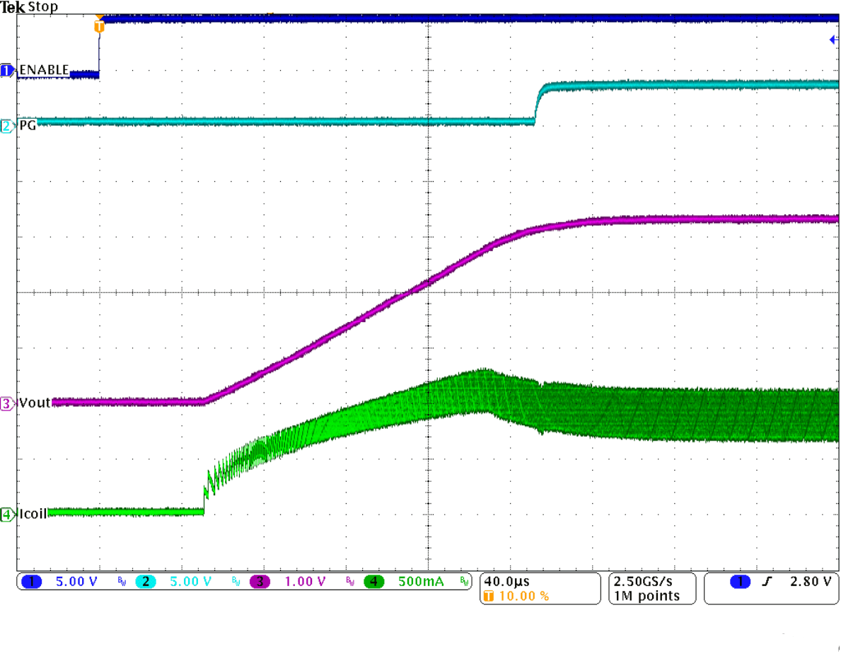
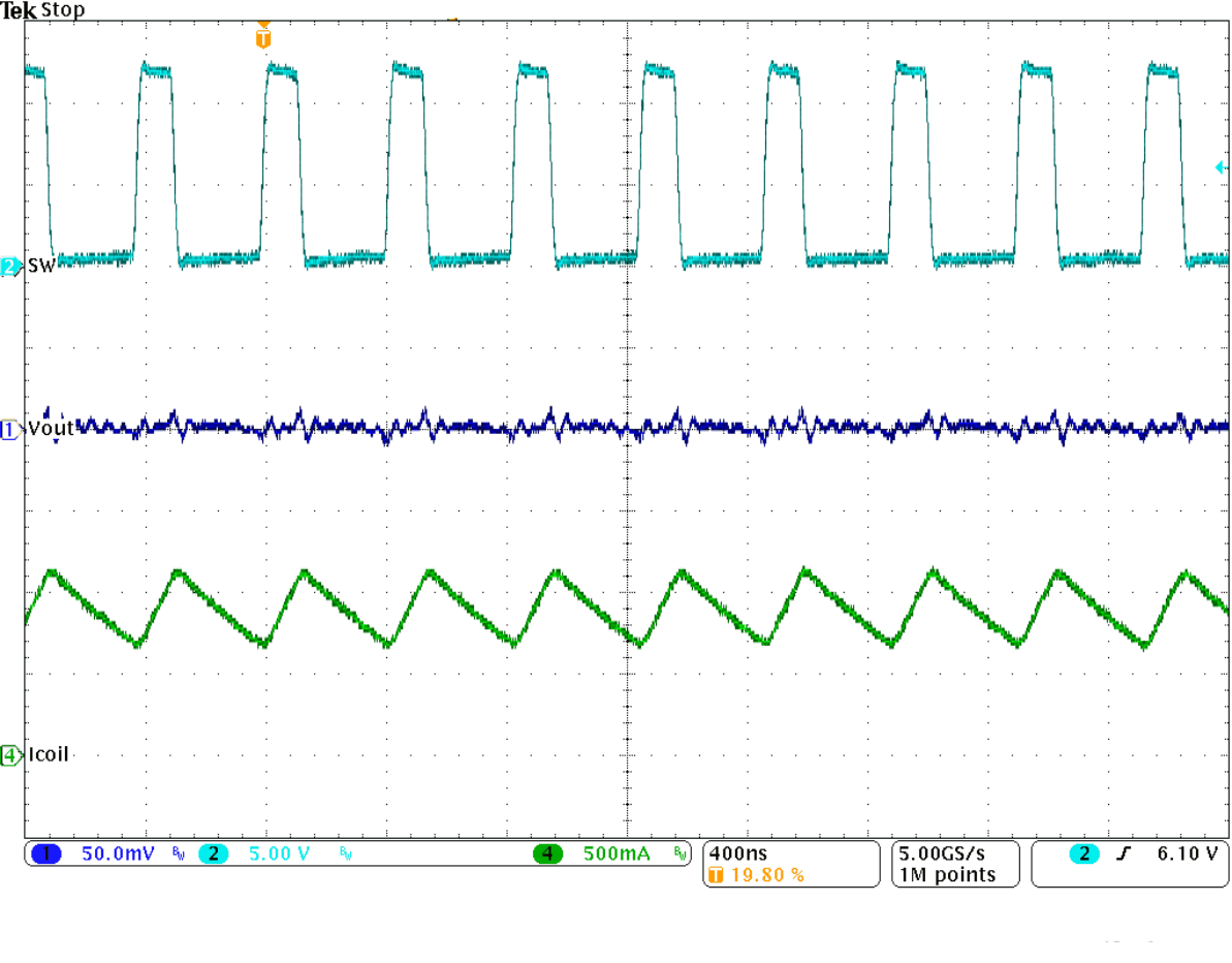
9.2.3 Application Performance Plots
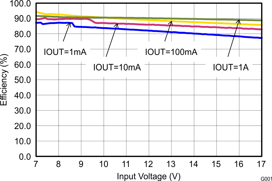
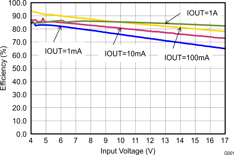
At VIN = 12 V, VOUT = 3.3 V and TJ = 25°C (unless otherwise noted)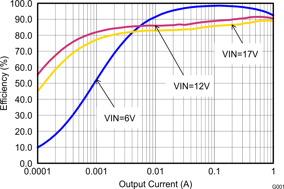
| Vout = 6 V | ||
| Vout = 3.3 V | ||
| Vout = 1.8 V | ||

| Vout = 0.9 V | ||
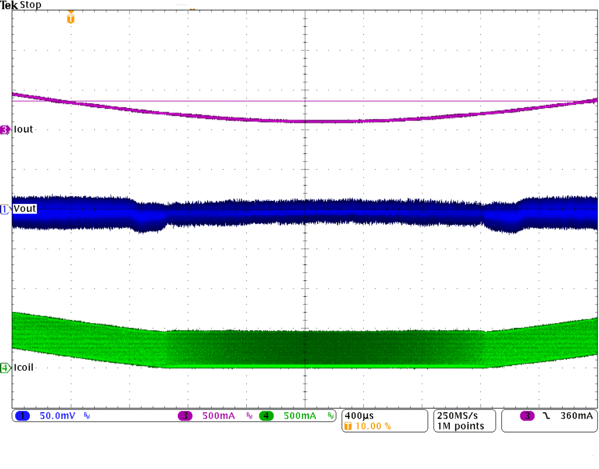
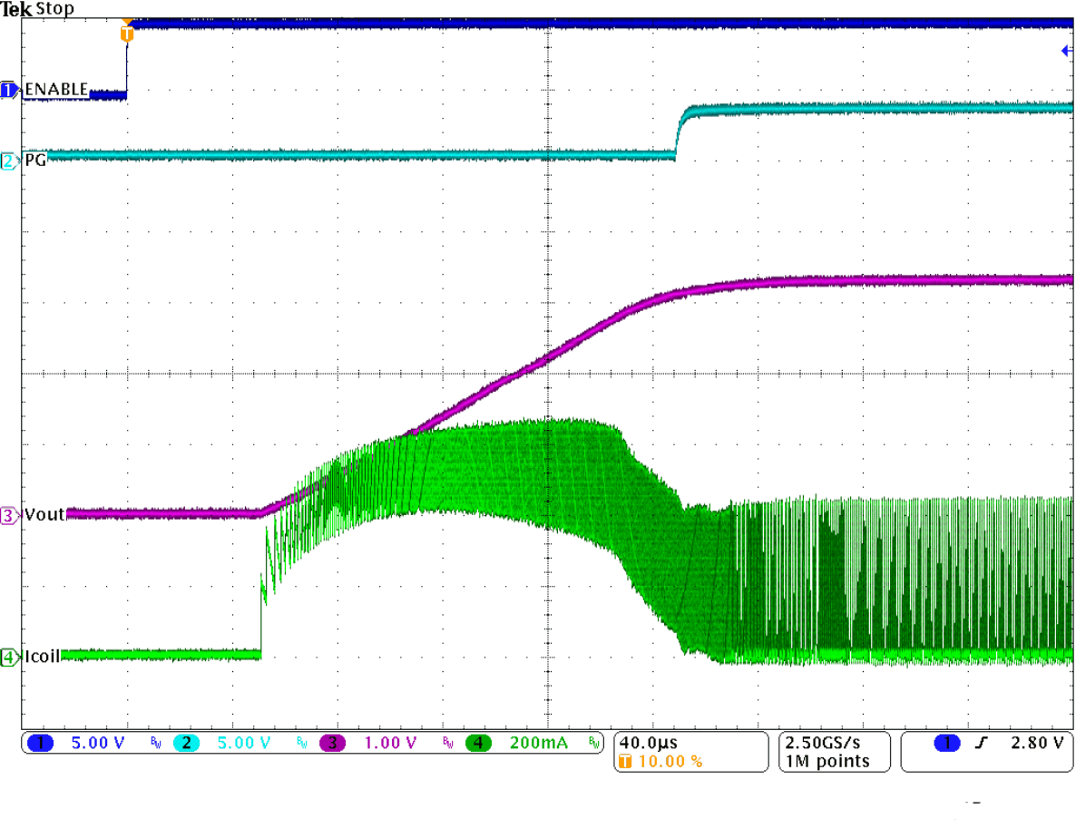
| 500 mA to 1 A |
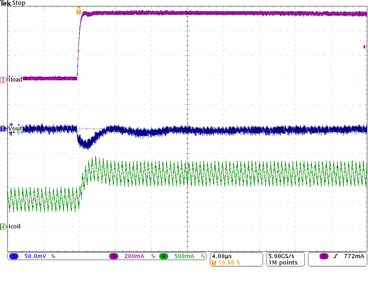
| 500 mA to 1 A, Rising edge | ||
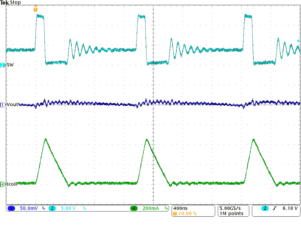
| Iout = 100 mA |
| Iout = 66 mA |
| Vout = 6 V | ||
| Vout = 3.3 V | ||
| Vout = 1.8 V | ||
| Vout = 0.9 V | ||
| 100 mA to 500 mA |
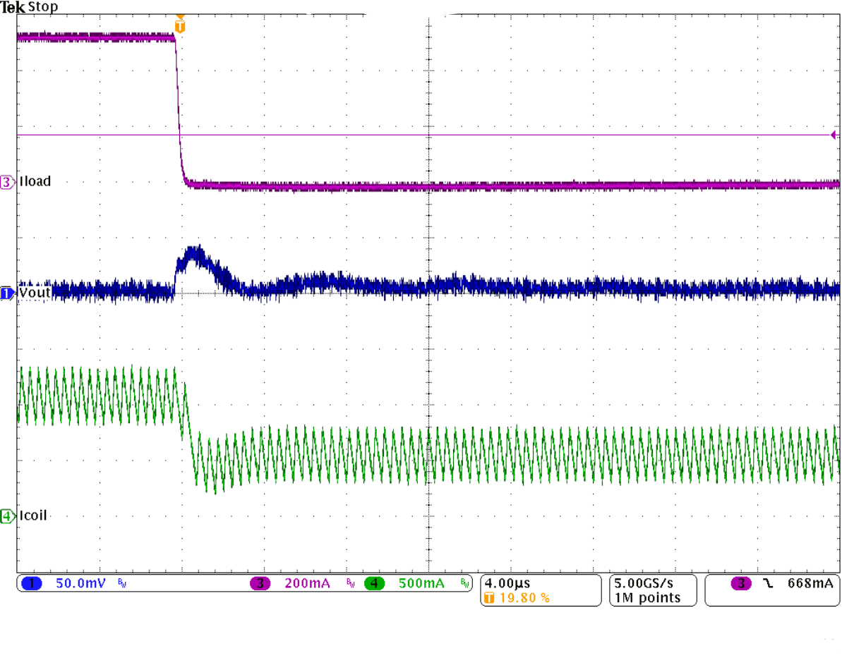
| 500 mA to 1 A, Falling edge | ||
| Iout = 1 A |
| Iout = 1 A |
9.3 System Examples
9.3.1 Inverting Power Supply
The TPS62160-Q1 can be used as inverting power supply by rearranging external circuitry as shown in Figure 30. As the former GND node now represents a voltage level below system ground, the voltage difference between VIN and VOUT has to be limited for operation to the maximum supply voltage of 17 V (see Equation 13).

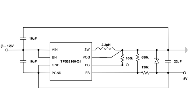 Figure 30. –5-V Inverting Power Supply
The transfer function of the inverting power supply configuration differs from the buck mode transfer function, incorporating a Right Half Plane Zero additionally. The loop stability has to be adapted and an output capacitance of at least 22 µF is recommended. A detailed design example is given in SLVA469.
9.3.2 Various Output Voltages
The TPS62160-Q1 can be set for different output voltages between 0.9 V and 6 V. Some examples are shown below.
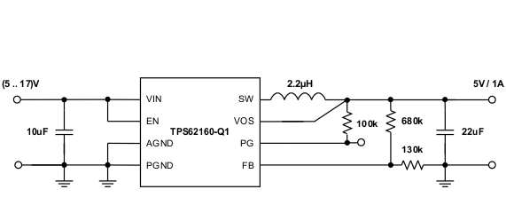 Figure 31. 5-V/1-A Power Supply
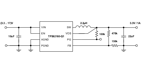 Figure 32. 3.3-V/1-A Power Supply
 Figure 33. 2.5-V/1-A Power Supply
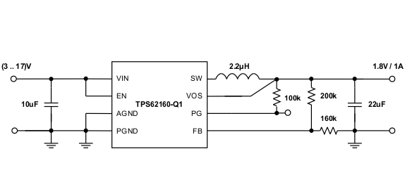 Figure 34. 1.8-V/1-A Power Supply
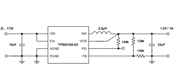 Figure 35. 1.5-V/1-A Power Supply
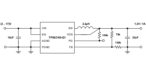 Figure 36. 1.2-V/1-A Power Supply
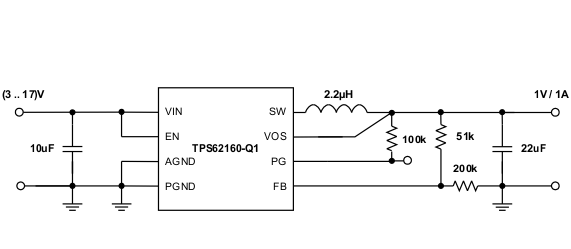 Figure 37. 1-V/1-A Power Supply