ZHCSD49 December 2014 TPS62160-Q1
PRODUCTION DATA.
- 1 特性
- 2 应用
- 3 说明
- 4 简化电路原理图
- 5 修订历史记录
- 6 Pin Configuration and Functions
- 7 Specifications
- 8 Detailed Description
- 9 Application and Implementation
- 10Power Supply Recommendations
- 11Layout
- 12器件和文档支持
- 13机械封装和可订购信息
6 Pin Configuration and Functions
8-Pin WSON
DSG Package
(Top View)
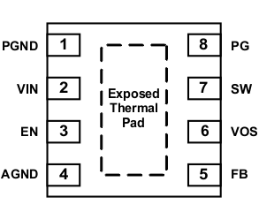
Pin Functions
| PIN(1) | I/O | DESCRIPTION | |
|---|---|---|---|
| NAME | NUMBER | ||
| PGND | 1 | Power ground | |
| VIN | 2 | I | Supply voltage |
| EN | 3 | I | Enable input (High = enabled, Low = disabled) |
| AGND | 4 | Analog Ground | |
| FB | 5 | I | Voltage feedback of adjustable version. Connect resistive voltage divider to this pin. It is recommended to connect FB to AGND on fixed output voltage versions for improved thermal performance. |
| VOS | 6 | I | Output voltage sense pin and connection for the control loop circuitry. |
| SW | 7 | O | Switch node, which is connected to the internal MOSFET switches. Connect inductor between SW and output capacitor. |
| PG | 8 | O | Output power good (High = VOUT ready, Low = VOUT below nominal regulation) ; open drain (requires pull-up resistor; goes high impedance, when device is switched off) |
| Exposed Thermal Pad | Must be connected to AGND. Must be soldered to achieve appropriate power dissipation and mechanical reliability. | ||
(1) For more information about connecting pins, see Detailed Description and Application Information sections.