ZHCSD49 December 2014 TPS62160-Q1
PRODUCTION DATA.
- 1 特性
- 2 应用
- 3 说明
- 4 简化电路原理图
- 5 修订历史记录
- 6 Pin Configuration and Functions
- 7 Specifications
- 8 Detailed Description
- 9 Application and Implementation
- 10Power Supply Recommendations
- 11Layout
- 12器件和文档支持
- 13机械封装和可订购信息
11 Layout
11.1 Layout Guidelines
A proper layout is critical for the operation of a switched mode power supply, even more at high switching frequencies. Therefore the PCB layout of the TPS62160-Q1 demands careful attention to ensure operation and to get the performance specified. A poor layout can lead to issues like poor regulation (both line and load), stability and accuracy weaknesses, increased EMI radiation and noise sensitivity. Considering the following topics ensures best electrical and optimized thermal performance:
1) The input capacitor must be placed as close as possible to the VIN and PGND pin of the IC. This provides low resistive and inductive path for the high di/dt input current.
2) The VOS pin must be connect in the shortest way to VOUT at the output capacitor - avoiding noise coupling.
3) The feedback resistors, R1 and R2 must be connected close to the FB and AGND pins - avoiding noise coupling.
4) The output capacitor should be placed such that its ground is as close as possible to the IC's PGND pins - avoiding additional voltage drop in traces.
5) The inductor should be placed close to the SW pin and connect directly to the output capacitor - minimizing the loop area between the SW pin, inductor, output capacitor and PGND pin.
More detailed information can be found in the EVM Users Guide, SLVU483.
The Exposed Thermal Pad must be soldered to the circuit board for mechanical reliability and to achieve appropriate power dissipation. Although the Exposed Thermal Pad can be connected to a floating circuit board trace, the device will have better thermal performance if it is connected to a larger ground plane. The Exposed Thermal Pad is electrically connected to AGND.
11.2 Layout Example
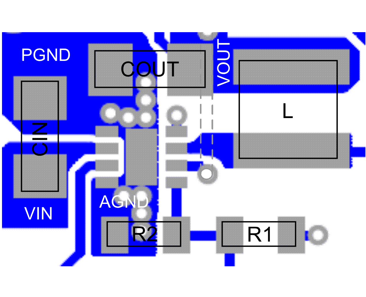 Figure 38. Layout Example
11.3 Thermal Considerations
Implementation of integrated circuits in low-profile and fine-pitch surface-mount packages typically requires special attention to power dissipation. Many system-dependent issues such as thermal coupling, airflow, added heat sinks and convection surfaces, and the presence of other heat-generating components affect the power-dissipation limits of a given component.
Three basic approaches for enhancing thermal performance are listed below:
- Improving the power dissipation capability of the PCB design
- Improving the thermal coupling of the component to the PCB by soldering the Exposed Thermal Pad
- Introducing airflow in the system
For more details on how to use the thermal parameters, see the application notes: Thermal Characteristics Application Note (SZZA017), and (SPRA953).
The TPS62160-Q1 is designed for a maximum operating junction temperature (TJ) of 125°C. Therefore the maximum output power is limited by the power losses that can be dissipated over the actual thermal resistance, given by the package and the surrounding PCB structures. Since the thermal resistance of the package is fixed, increasing the size of the surrounding copper area and improving the thermal connection to the IC can reduce the thermal resistance. To get an improved thermal behavior, it's recommended to use top layer metal to connect the device with wide and thick metal lines. Internal ground layers can connect to vias directly under the IC for improved thermal performance.
If short circuit or overload conditions are present, the device is protected by limiting internal power dissipation.