ZHCSBB4B July 2013 – June 2017 TPS61197
PRODUCTION DATA.
- 1 特性
- 2 应用范围
- 3 说明
- 4 修订历史记录
- 5 Pin Configuration and Functions
- 6 Specifications
-
7 Detailed Description
- 7.1 Overview
- 7.2 Functional Block Diagram
- 7.3 Feature Description
- 7.4
Device Functional Modes
- 7.4.1
Protections
- 7.4.1.1 Switch Current Limit Protection Using the ISNS Pin
- 7.4.1.2 LED Open Protection
- 7.4.1.3 Schottky Diode Open Protection
- 7.4.1.4 Schottky Diode Short Protection
- 7.4.1.5 IFB Overvoltage Protection
- 7.4.1.6 Output Overvoltage Protection Using the OVP Pin
- 7.4.1.7 IFB Short-to-Ground Protection
- 7.4.1.8 Thermal Shutdown
- 7.4.1
Protections
- 8 Application and Implementation
- 9 Power Supply Recommendations
- 10Layout
- 11器件和文档支持
- 12机械、封装和可订购信息
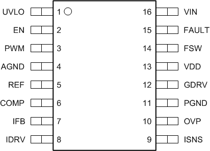
5 Pin Configuration and Functions
D Package
16-Pin SOIC
Top View

Pin Functions
| PIN | TYPE | DESCRIPTION | |
|---|---|---|---|
| NO. | NAME | ||
| 1 | UVLO | I | Low input undervoltage lockout. Use a resister divider from VIN to this pin to set the UVLO threshold. |
| 2 | EN | I | Device enable and disable control input. EN pin high voltage enables the device. EN pin low voltage disables the device. |
| 3 | PWM | I | PWM dimming signal input. The frequency of the PWM signal is in the range of 90 Hz to 22 kHz. |
| 4 | AGND | G | Analog ground |
| 5 | REF | O | Internal reference voltage for the boost converter. Use a capacitor at this pin to adjust the soft-start time. |
| 6 | COMP | O | Loop compensation for the boost converter. Connect a RC network to make loop stable |
| 7 | IFB | I | Regulated current sink input pin. A resistor on this pin is used to set a desired string current. |
| 8 | IDRV | O | PWM dimming output control pin to drive the external MOSFET or bipolar transistor |
| 9 | ISNS | I | External switch MOSFET current sense positive input |
| 10 | OVP | I | Overvoltage protection detection input. Connect a resistor divider from output to this pin to program the OVP threshold. In addition, this pin is also the feedback of the output voltage of the boost converter. |
| 11 | PGND | G | External MOSFET current sense ground input |
| 12 | GDRV | O | Gate driver output for the external switch MOSFET |
| 13 | VDD | O | Internal regulator output for device power supply. Connect a ceramic capacitor of more than 1 µF to this pin. |
| 14 | FSW | O | Boost switching frequency setting pin. Use a resistor to set the frequency from 50 kHz to 800 kHz. |
| 15 | FAULT | O | Fault indicator. Open-drain output. Output high impedance when fault conditions happen. |
| 16 | VIN | I | Power supply input pin |