ZHCSBB4B July 2013 – June 2017 TPS61197
PRODUCTION DATA.
- 1 特性
- 2 应用范围
- 3 说明
- 4 修订历史记录
- 5 Pin Configuration and Functions
- 6 Specifications
-
7 Detailed Description
- 7.1 Overview
- 7.2 Functional Block Diagram
- 7.3 Feature Description
- 7.4
Device Functional Modes
- 7.4.1
Protections
- 7.4.1.1 Switch Current Limit Protection Using the ISNS Pin
- 7.4.1.2 LED Open Protection
- 7.4.1.3 Schottky Diode Open Protection
- 7.4.1.4 Schottky Diode Short Protection
- 7.4.1.5 IFB Overvoltage Protection
- 7.4.1.6 Output Overvoltage Protection Using the OVP Pin
- 7.4.1.7 IFB Short-to-Ground Protection
- 7.4.1.8 Thermal Shutdown
- 7.4.1
Protections
- 8 Application and Implementation
- 9 Power Supply Recommendations
- 10Layout
- 11器件和文档支持
- 12机械、封装和可订购信息
7.3.5 Power-Up Sequencing and Soft Start-up
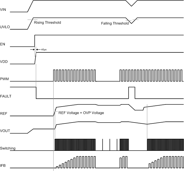
The input voltage, UVLO pin voltage, EN input signal, and the input dimming PWM signal control the power up of the TPS61197. After the input voltage is above the required minimal input voltage of 7.5 V, the internal circuit is ready to be powered up. After the UVLO pin voltage is above the threshold of 1.229 V and the EN signal is high, the internal LDO and logic circuit are activated. When the PWM dimming signal is high, the soft start-up begins.
 Figure 16. Power-Up Sequencing
The TPS61197 has integrated the soft-start circuitry working with an external capacitor at the REF pin to avoid inrush current during start-up. During the start-up period, the capacitor at the REF pin is charged with a soft-start current source. When the REF pin voltage is higher than the output feedback voltage at the OVP pin, the boost controller starts switching, and the output voltage starts to ramp up. At the same time, the LED current regulation circuit starts to drive the LED string. At the beginning of the soft start, the charge current is 200 µA. Once the voltage of the REF pin exceeds 2 V, the charge current stops. The output voltage continues to ramp up until the IFB voltage is in regulation of 300 mV. The total soft-start time is determined by the external capacitance at the REF pin. The capacitance must be within 470 nF to 4.7 µF for different start-up time.
 Figure 17. Soft-Start Waveforms