ZHCSD56 December 2014 TPS61175-Q1
PRODUCTION DATA.
- 1 特性
- 2 应用范围
- 3 说明
- 4 简化电路原理图
- 5 修订历史记录
- 6 Pin Configuration and Functions
- 7 Specifications
- 8 Detailed Description
-
9 Application and Implementation
- 9.1 Application Information
- 9.2
Typical Application
- 9.2.1 Design Requirements
- 9.2.2
Detailed Design Procedure
- 9.2.2.1 Determining the Duty Cycle
- 9.2.2.2 Selecting the Inductor
- 9.2.2.3 Computing the Maximum Output Current
- 9.2.2.4 Setting Output Voltage
- 9.2.2.5 Setting the Switching Frequency
- 9.2.2.6 Setting the Soft Start Time
- 9.2.2.7 Selecting the Schottky Diode
- 9.2.2.8 Selecting the Input and Output Capacitors
- 9.2.2.9 Compensating the Small Signal Control Loop
- 9.2.3 Application Curves
- 10Power Supply Recommendations
- 11Layout
- 12器件和文档支持
- 13机械封装和可订购信息
9 Application and Implementation
9.1 Application Information
The following section provides a step-by-step design approach for configuring the TPS61175-Q1 as a voltage regulating boost converter, as shown in Figure 8. When configured as SEPIC or flyback converter, a different design approach is required.
9.2 Typical Application
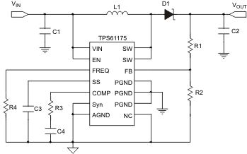 Figure 8. Boost Converter Configuration
9.2.1 Design Requirements
Table 3. Design Parameters
| PARAMETERS | VALUES |
|---|---|
| Input voltage | 5 V |
| Output voltage | 24 V |
| Operating frequency | 1.2 MHz |
9.2.2 Detailed Design Procedure
9.2.2.1 Determining the Duty Cycle
The TPS61175-Q1 has a maximum worst case duty cycle of 89% and a minimum on time of 60 ns. These two constraints place limitations on the operating frequency that can be used for a given input to output conversion ratio. The duty cycle at which the converter operates is dependent on the mode in which the converter is running. If the converter is running in discontinuous conduction mode (DCM), where the inductor current ramps to zero at the end of each cycle, the duty cycle varies with changes to the load much more than it does when running in continuous conduction mode (CCM). In continuous conduction mode, where the inductor maintains a dc current, the duty cycle is related primarily to the input and output voltages as computed below:
In discontinuous mode the duty cycle is a function of the load, input and output voltages, inductance and switching frequency as computed below:
All converters using a diode as the freewheeling or catch component have a load current level at which they transition from discontinuous conduction to continuous conduction. This is the point where the inductor current just falls to zero. At higher load currents, the inductor current does not fall to zero but remains flowing in a positive direction and assumes a trapezoidal wave shape as opposed to a triangular wave shape. This load boundary between discontinuous conduction and continuous conduction can be found for a set of converter parameters as follows.
For loads higher than the result of the equation above, the duty cycle is given by Equation 3 and for loads less than the results of Equation 4, the duty cycle is given in Equation 5. For Equation 3 through Equation 5, the variable definitions are as follows.
- VOUT is the output voltage of the converter in V
- VD is the forward conduction voltage drop across the rectifier or catch diode in V
- VIN is the input voltage to the converter in V
- IOUT is the output current of the converter in A
- L is the inductor value in H
- fSW is the switching frequency in Hz
Unless otherwise stated, the design equations that follow assume that the converter is running in continuous mode.
9.2.2.2 Selecting the Inductor
The selection of the inductor affects steady state operation as well as transient behavior and loop stability. These factors make it the most important component in power regulator design. There are three important inductor specifications, inductor value, DC resistance and saturation current. Considering inductor value alone is not enough.
Inductor values can have ±20% tolerance with no current bias. When the inductor current approaches saturation level, its inductance can fall to some percentage of its 0-A value depending on how the inductor vendor defines saturation current. For CCM operation, the rule of thumb is to choose the inductor so that its inductor ripple current (ΔIL) is no more than a certain percentage (RPL% = 20–40%) of its average DC value (IIN(AVG) = IL(AVG))
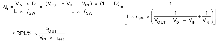
Rearranging and solving for L gives
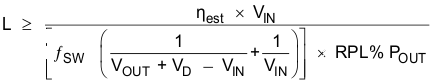
Choosing the inductor ripple current to closer to 20% of the average inductor current results in a larger inductance value, maximizes the converter’s potential output current and minimizes EMI. Choosing the inductor ripple current closer to 40% of IL(AVG) results in a smaller inductance value, and a physically smaller inductor, improves transient response but results in potentially higher EMI and lower efficiency if the DCR of the smaller packaged inductor is significantly higher. Using an inductor with a smaller inductance value than computed above may result in the converter operating in DCM. This reduces the boost converter’s maximum output current, causes larger input voltage and output ripple and typically reduces efficiency. Table 4 lists the recommended inductor for the TPS61175-Q1.
Table 4. Recommended Inductors for TPS61175-Q1
| PART NUMBER | L (μH) |
DCR MAX (mΩ) |
SATURATION CURRENT (A) |
SIZE (L × W × H mm) |
VENDOR |
|---|---|---|---|---|---|
| D104C2 | 10 | 44 | 3.6 | 10.4x10.4x4.8 | TOKO |
| VLF10040 | 15 | 42 | 3.1 | 10.0x9.7x4.0 | TDK |
| CDRH105RNP | 22 | 61 | 2.9 | 10.5x10.3x5.1 | Sumida |
| MSS1038 | 15 | 50 | 3.8 | 10.0x10.2x3.8 | Coilcraft |
The device has built-in slope compensation to avoid subharmonic oscillation associated with current mode control. If the inductor value is lower than 4.7μH, the slope compensation may not be adequate, and the loop can be unstable. Applications requiring inductors above 47μH have not been evaluated. Therefore, the user is responsible for verifying operation if they select an inductor that is outside the 4.7μH–47μH recommended range.
9.2.2.3 Computing the Maximum Output Current
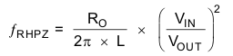
The over-current limit for the integrated power FET limits the maximum input current and thus the maximum input power for a given input voltage. Maximum output power is less than maximum input power due to power conversion losses. Therefore, the current limit setting, input voltage, output voltage and efficiency can all change the maximum current output (IOUT(MAX)). The current limit clamps the peak inductor current, therefore the ripple has to be subtracted to derive maximum DC current.
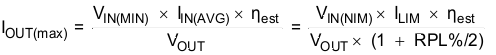
where
- ILIM = over current limit
- ηest= efficiency estimate based on similar applications or computed above
For instance, when VIN = 12 V is boosted to VOUT = 24 V, the inductor is 10 uH, the Schottky forward voltage is 0.4-V and the switching frequency is 1.2-MHz; then the maximum output current is 1.2-A in typical condition, assuming 90% efficiency and a %RPL = 20%.
9.2.2.4 Setting Output Voltage
To set the output voltage in either DCM or CCM, select the values of R1 and R2 according to the following equation.
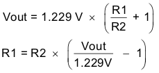
Considering the leakage current through the resistor divider and noise decoupling into FB pin, an optimum value for R2 is around 10k. The output voltage tolerance depends on the VFB accuracy and the tolerance of R1 and R2.
9.2.2.5 Setting the Switching Frequency
Choose the appropriate resistor from the resistance versus frequency table Table 1 or graph Figure 7. A resistor must be placed from the FREQ pin to ground, even if an external oscillation is applied for synchronization.
Increasing switching frequency reduces the value of external capacitors and inductors, but also reduces the power conversion efficiency. The user should set the frequency for the minimum tolerable efficiency.
9.2.2.6 Setting the Soft Start Time
Choose the appropriate capacitor from the soft start table Table 2. Increasing the soft start time reduces the overshoot during start-up.
9.2.2.7 Selecting the Schottky Diode
The high switching frequency of the TPS61175-Q1 demands a high-speed rectification for optimum efficiency. Ensure that the diode’s average and peak current rating exceed the average output current and peak inductor current. In addition, the diode’s reverse breakdown voltage must exceed the switch FET rating voltage of 40V. So, the VISHAY SS3P6L-E3/86A is recommended for TPS61175-Q1. The power dissipation of the diode's package must be larger than IOUT(max) x VD
9.2.2.8 Selecting the Input and Output Capacitors
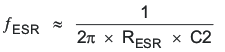
The output capacitor is mainly selected to meet the requirements for the output ripple and load transient. Then the loop is compensated for the output capacitor selected. The output ripple voltage is related to the capacitor’s capacitance and its equivalent series resistance (ESR). Assuming a capacitor with zero ESR, the minimum capacitance needed for a given ripple can be calculated by
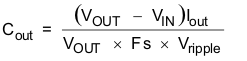
where, Vripple= peak to peak output ripple. The additional output ripple component caused by ESR is calculated using:
Vripple_ESR = I × RESR
Due to its low ESR, Vripple_ESR can be neglected for ceramic capacitors, but must be considered if tantalum or electrolytic capacitors are used.
The minimum ceramic output capacitance needed to meet a load transient requirement can be estimated by Equation 11.
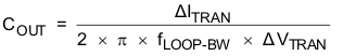
Where
- ΔITRAN is the transient load current step
- ΔVTRAN is the allowed voltage dip for the load current step
- fLOOP-BW is the control loop bandwidth (that is, the frequency where the control loop gain crosses zero).
Care must be taken when evaluating a ceramic capacitor’s derating under dc bias, aging and AC signal. For example, larger form factor capacitors (in 1206 size) have their self resonant frequencies in the range of the switching frequency. So the effective capacitance is significantly lower. The DC bias can also significantly reduce capacitance. Ceramic capacitors can loss as much as 50% of its capacitance at its rated voltage. Therefore, one must add margin on the voltage rating to ensure adequate capacitance at the required output voltage.
For a typical boost converter implementation, at least 4.7μF of ceramic input and output capacitance is recommended. Additional input and output capacitance may be required to meet ripple and/or transient requirements.
The popular vendors for high value ceramic capacitors are:
TDK (http://www.component.tdk.com/components.php)
Murata (http://www.murata.com/cap/index.html)
9.2.2.9 Compensating the Small Signal Control Loop
All continuous mode boost converters have a right half plane zero (ƒRHPZ) due to the inductor being removed from the output during charging. In a traditional voltage mode controlled boost converter, the inductor and output capacitor form a small signal double pole. For a negative feedback system to be stable, the fed back signal must have a gain less than 1 before having 180 degrees of phase shift. With its double pole and RHPZ all providing phase shift, voltage mode boost converters are a challenge to compensate. In a converter with current mode control, there are essentially two loops, an inner current feedback loop created by the inductor current information sensed across RSENSE (40 mΩ) and the output voltage feedback loop. The inner current loop allows the switch, inductor and modulator to be lumped together into a small signal variable current source controlled by the error amplifier, as shown in Figure 9.
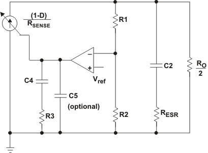 Figure 9. Small Signal Model of a Current Mode Boost in CCM
The new power stage, including the slope compensation, small signal model becomes:
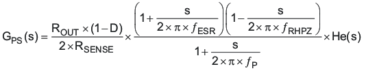
Where
And
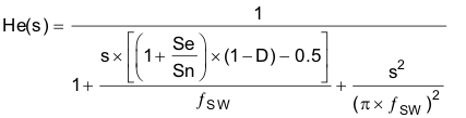
He(s) models the inductor current sampling effect as well as the slope compensation effect on the small signal response.
NOTE
If Se slope dominates Sn, that is, when the inductance is oversized in order to give ripple current much smaller than the recommended 0.2 – 0.4 times the average input current, then the converter behaves more like a voltage mode converter, and the above model no longer holds.
The slope compensation in TPS61175-Q1 is shown as follow
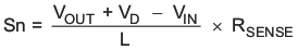
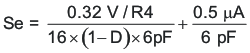
Figure 10 shows a bode plot of a typical CCM boost converter power stage
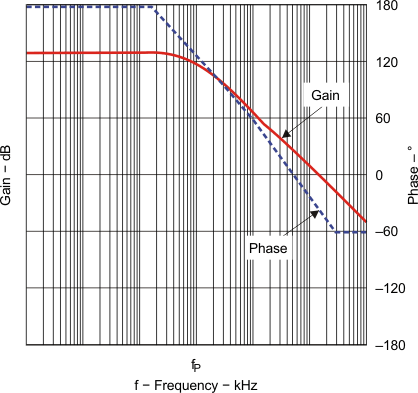 Figure 10. Bode Plot of Power Stage Gain and Phase
The TPS61175-Q1 COMP pin is the output of the internal trans-conductance amplifier. Equation 19 shows the equation for feedback resistor network and the error amplifier.
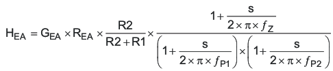
where GEA and REA are the amplifier’s trans-conductance and output resistance located in the Electrical Characteristics table.
and
Figure 11 shows a typical bode plot for transfer function H(s).
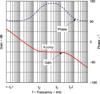 Figure 11. Bode Plot of Feedback Resistors and Compensated Amplifier Gain and Phase
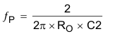
The next step is to choose the loop crossover frequency, fC. The higher in frequency that the loop gain stays above zero before crossing over, the faster the loop response will be and therefore the lower the output voltage will droop during a step load. It is generally accepted that the loop gain cross over no higher than the lower of either 1/5 of the switching frequency, fSW, or 1/3 of the RHPZ frequency, fRHPZ. To approximate a single pole roll-off up to fP2, select R3 so that the compensation gain, KCOMP, at fC on Figure 11 is the reciprocal of the gain, KPW, read at frequency fC from the Figure 10 bode plot or more simply
KCOMP(fC) = 20 × log(GEA × R3 × R2/(R2+R1)) = 1/KPW(fC)
This makes the total loop gain, T(s) = GPS(s) × HEA(s), zero at the fC. Then, select C4 so that fZ ≅ fC/10 and optional fP2> fC *10. Following this method should lead to a loop with a phase margin near 45 degrees. Lowering R3 while keeping fZ ≅ fC/10 increases the phase margin and therefore increases the time it takes for the output voltage to settle following a step load.
In the TPS61175-Q1, if the FB pin voltage changes suddenly due to a load step on the output voltage, the error amplifier increases its transconductance for 8-ms in an effort to speed up the IC’s transient response and reduce output voltage droop due to the load step. For example, if the FB voltage decreases 10-mV due to load change, the error amplifier increases its source current through COMP by 5 times; if FB voltage increases 11-mV, the sink current through COMP is increased to 3.5 times normal value. This feature often results in saw tooth ringing on the output voltage, shown as Figure 13. Designing the loop for greater than 45 degrees of phase margin and greater than 10db gain margin minimizes the amplitude of this ringing. This feature is disabled during soft start.
9.2.3 Application Curves
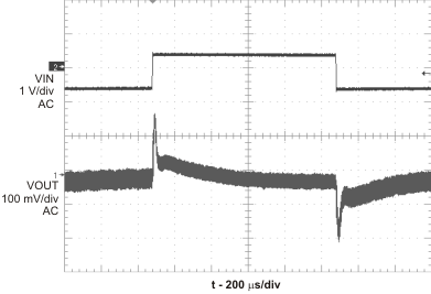 Figure 12. Line Transient Response
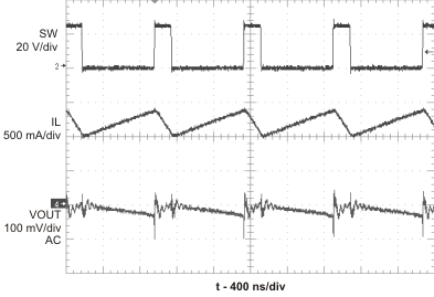 Figure 14. PWM Operation
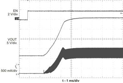 Figure 16. Soft Startup
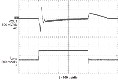 Figure 13. Load Transient Response
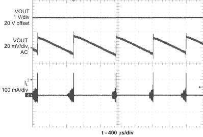 Figure 15. Pulse Skipping