ZHCSD56 December 2014 TPS61175-Q1
PRODUCTION DATA.
- 1 特性
- 2 应用范围
- 3 说明
- 4 简化电路原理图
- 5 修订历史记录
- 6 Pin Configuration and Functions
- 7 Specifications
- 8 Detailed Description
-
9 Application and Implementation
- 9.1 Application Information
- 9.2
Typical Application
- 9.2.1 Design Requirements
- 9.2.2
Detailed Design Procedure
- 9.2.2.1 Determining the Duty Cycle
- 9.2.2.2 Selecting the Inductor
- 9.2.2.3 Computing the Maximum Output Current
- 9.2.2.4 Setting Output Voltage
- 9.2.2.5 Setting the Switching Frequency
- 9.2.2.6 Setting the Soft Start Time
- 9.2.2.7 Selecting the Schottky Diode
- 9.2.2.8 Selecting the Input and Output Capacitors
- 9.2.2.9 Compensating the Small Signal Control Loop
- 9.2.3 Application Curves
- 10Power Supply Recommendations
- 11Layout
- 12器件和文档支持
- 13机械封装和可订购信息
7 Specifications
7.1 Absolute Maximum Ratings(1)
over operating free-air temperature range (unless otherwise noted)| VALUE | UNIT | ||
|---|---|---|---|
| MIN | MAX | ||
| Supply Voltages on pin VIN (2) | –0.3 | 20 | V |
| Voltages on pins EN(2) | –0.3 | 20 | V |
| Voltage on pin FB, FREQ and COMP(2) | –0.3 | 3 | V |
| Voltage on pin SYNC, SS(2) | –0.3 | 7 | V |
| Voltage on pin SW(2) | –0.3 | 40 | V |
| Continuous Power Dissipation | See the Thermal Information Table | ||
| Operating Junction Temperature Range | –40 | 150 | °C |
| Storage temperature, Tstg | –65 | 150 | °C |
(1) Stresses beyond those listed under "absolute maximum ratings" may cause permanent damage to the device. These are stress ratings only and functional operation of the device at these or any other conditions beyond those indicated under "recommended operating conditions" is not implied. Exposure to absolute-maximum-rated conditions for extended periods may affect device reliability.
(2) All voltage values are with respect to network ground terminal.
7.2 ESD Ratings
| VALUE | UNIT | ||||
|---|---|---|---|---|---|
| V(ESD) | Electrostatic discharge | Human-body model (HBM), per AEC Q100-002(1) | ±2000 | V | |
| Charged-device model (CDM), per AEC Q100-011 | All pins except 1, 7, 8, and 14 | ±500 | |||
| Pins 1, 7, 8, and 14 | ±750 | ||||
(1) AEC Q100-002 indicates that HBM stressing shall be in accordance with the ANSI/ESDA/JEDEC JS-001 specification.
7.3 Recommended Operating Conditions
over operating free-air temperature range (unless otherwise noted)| MIN | NOM | MAX | UNIT | ||
|---|---|---|---|---|---|
| VIN | Input voltage range | 2.9 | 18 | V | |
| VO | Output voltage range | VIN | 38 | V | |
| L | Inductor(1) | 4.7 | 47 | μH | |
| fSW | Switching frequency | 200 | 2200 | kHz | |
| CI | Input Capacitor | 4.7 | μF | ||
| CO | Output Capacitor | 4.7 | μF | ||
| VSYN | External Switching Frequency Logic | 5 | V | ||
| TA | Operating ambient temperature | –40 | 125 | °C | |
| TJ | Operating junction temperature | –40 | 125 | °C | |
(1) The inductance value depends on the switching frequency and end application. While larger values may be used, values between 4.7-μH and 47-μH have been successfully tested in various applications. Refer to the Inductor Selection for detail.
7.4 Thermal Information
| THERMAL METRIC(1) | TPS61175-Q1 | UNIT | |
|---|---|---|---|
| PWP | |||
| 14 PINS | |||
| RθJA | Junction-to-ambient thermal resistance | 45.2 | °C/W |
| RθJC(top) | Junction-to-case (top) thermal resistance | 34.9 | |
| RθJB | Junction-to-board thermal resistance | 30.1 | |
| ψJT | Junction-to-top characterization parameter | 1.5 | |
| ψJB | Junction-to-board characterization parameter | 29.9 | |
| RθJC(bot) | Junction-to-case (bottom) thermal resistance | 5.8 | |
(1) For more information about traditional and new thermal metrics, see the IC Package Thermal Metrics application report, SPRA953.
7.5 Electrical Characteristics
FSW = 1.2 MHz (Rfreq = 80 kΩ), VIN = 3.6V, TA = TJ = –40°C to 125°C, typical values are at TA = 25°C (unless otherwise noted)| PARAMETER | TEST CONDITIONS | MIN | TYP | MAX | UNIT | |
|---|---|---|---|---|---|---|
| SUPPLY CURRENT | ||||||
| VIN | Input voltage range | 2.9 | 18 | V | ||
| IQ | Operating quiescent current into Vin | Device PWM switching without load | 3.5 | mA | ||
| ISD | Shutdown current | EN = GND | 1.5 | μA | ||
| VUVLO | Under-voltage lockout threshold | 2.5 | 2.7 | V | ||
| Vhys | Under-voltage lockout hysteresis | 130 | mV | |||
| ENABLE AND REFERENCE CONTROL | ||||||
| V(ENh) | EN logic high voltage | VIN = 2.9 V to 18 V | 1.2 | V | ||
| V(ENl) | EN logic low voltage | VIN = 2.9 V to 18 V | 0.4 | V | ||
| V(SYNh) | SYN logic high voltage | 1.2 | V | |||
| V(SYNl) | SYN logic low voltage | 0.4 | V | |||
| R(EN) | EN pull down resistor | 400 | 800 | 1600 | kΩ | |
| VOLTAGE AND CURRENT CONTROL | ||||||
| VREF | Voltage feedback regulation voltage | 1.204 | 1.229 | 1.254 | V | |
| IFB | Voltage feedback input bias current | 200 | nA | |||
| Isink | Comp pin sink current | VFB = VREF + 200 mV, VCOMP = 1 V | 50 | μA | ||
| Isource | Comp pin source current | VFB = VREF –200 mV, VCOMP = 1 V | 130 | μA | ||
| VCCLP | Comp pin Clamp Voltage | High Clamp, VFB = 1 V Low Clamp, VFB = 1.5 V |
3 0.75 |
V | ||
| V(CTH) | Comp pin threshold | Duty cycle = 0% | 0.95 | V | ||
| Gea | Error amplifier transconductance | 240 | 340 | 440 | μmho | |
| Rea | Error amplifier output resistance | 10 | MΩ | |||
| fea | Error amplifier crossover frequency | 500 | KHz | |||
| FREQUENCY | ||||||
| fS | Oscillator frequency | Rfreq = 480 kΩ | 0.16 | 0.21 | 0.26 | MHz |
| Rfreq = 80 kΩ | 1.0 | 1.2 | 1.4 | |||
| Rfreq = 40 kΩ | 1.76 | 2.2 | 2.64 | |||
| Dmax | Maximum duty cycle | VFB = 1.0 V, Rfreq = 80 kΩ | 89% | 93% | ||
| V(FREQ) | FREQ pin voltage | 1.229 | V | |||
| POWER SWITCH | ||||||
| RDS(ON) | N-channel MOSFET on-resistance | VIN = VGS = 3.6 V VIN = VGS = 3.0 V |
0.13 0.13 |
0.25 0.3 |
Ω | |
| ILN_NFET | N-channel leakage current | VDS = 40 V, TA = 25°C | 1 | μA | ||
| OC, OVP AND SS | ||||||
| ILIM | N-Channel MOSFET current limit | D = Dmax | 3 | 3.8 | 5 | A |
| ISS | Soft start bias current | VSS = 0 V | 6 | μA | ||
| THERMAL SHUTDOWN | ||||||
| Tshutdown | Thermal shutdown threshold | 160 | °C | |||
| Thysteresis | Thermal shutdown threshold hysteresis | 15 | °C | |||
7.6 Timing Requirements
| MIN | TYP | MAX | UNIT | |||
|---|---|---|---|---|---|---|
| ENABLE AND REFERENCE CONTROL | ||||||
| toff | Shutdown delay, SS discharge | EN high to low | 10 | ms | ||
| FREQUENCY | ||||||
| tmin_on | Minimum on pulse width | Rfreq = 80 kΩ | 60 | ns | ||
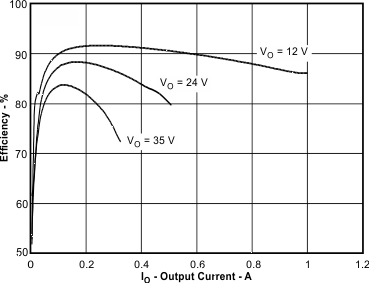
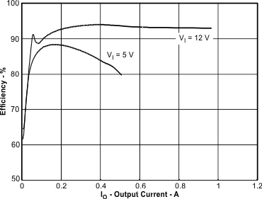
7.7 Typical Characteristics
| VI = 5 V |
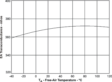 Figure 3. Error Amplifier Transconductance vs Free-Air Temperature
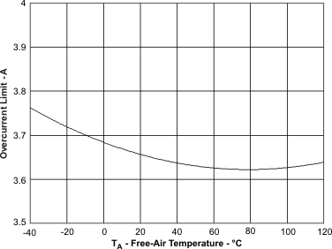 Figure 5. Overcurrent Limit vs Free-Air Temperature
| VO = 24 V |
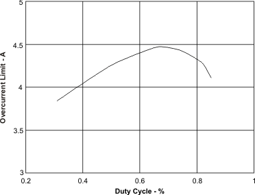 Figure 4. Overcurrent Limit vs Duty Cycle
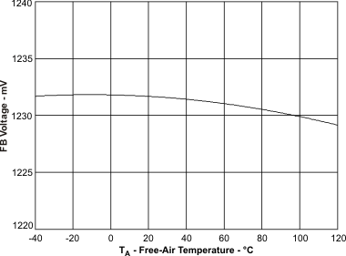 Figure 6. FB Voltages Free-Air Temperature