ZHCSD56 December 2014 TPS61175-Q1
PRODUCTION DATA.
- 1 特性
- 2 应用范围
- 3 说明
- 4 简化电路原理图
- 5 修订历史记录
- 6 Pin Configuration and Functions
- 7 Specifications
- 8 Detailed Description
-
9 Application and Implementation
- 9.1 Application Information
- 9.2
Typical Application
- 9.2.1 Design Requirements
- 9.2.2
Detailed Design Procedure
- 9.2.2.1 Determining the Duty Cycle
- 9.2.2.2 Selecting the Inductor
- 9.2.2.3 Computing the Maximum Output Current
- 9.2.2.4 Setting Output Voltage
- 9.2.2.5 Setting the Switching Frequency
- 9.2.2.6 Setting the Soft Start Time
- 9.2.2.7 Selecting the Schottky Diode
- 9.2.2.8 Selecting the Input and Output Capacitors
- 9.2.2.9 Compensating the Small Signal Control Loop
- 9.2.3 Application Curves
- 10Power Supply Recommendations
- 11Layout
- 12器件和文档支持
- 13机械封装和可订购信息
8 Detailed Description
8.1 Overview
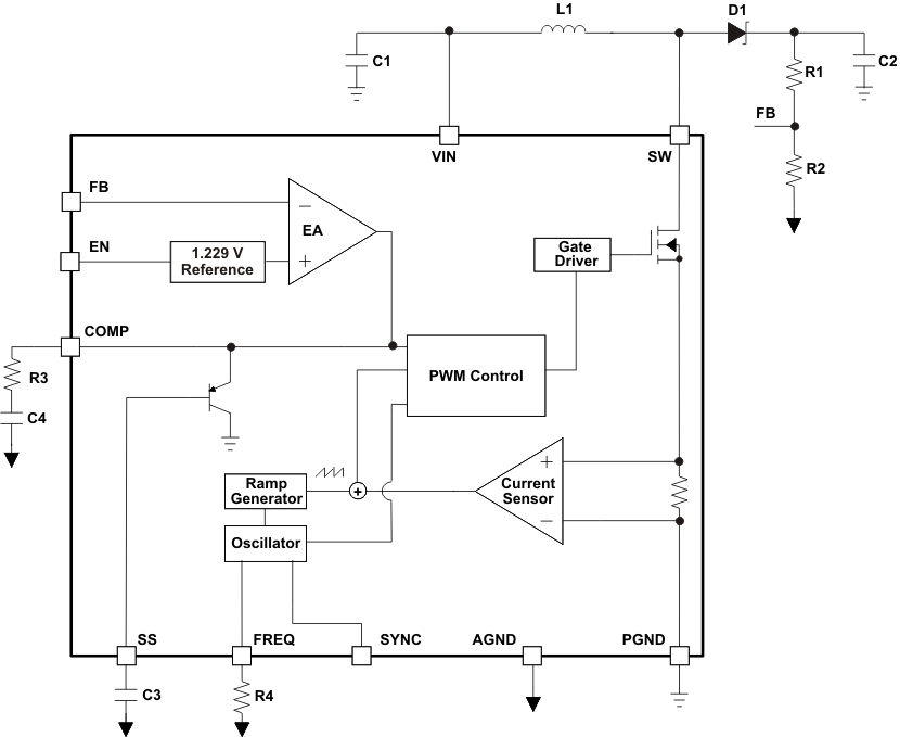
The TPS61175-Q1 integrates a 40-V low side switch FET for up to 38-V output. The device regulates the output with current mode PWM (pulse width modulation) control. The PWM control circuitry turns on the switch at the beginning of each switching cycle. The input voltage is applied across the inductor and stores the energy as inductor current ramps up. During this portion of the switching cycle, the load current is provided by the output capacitor. When the inductor current rises to the threshold set by the error amplifier output, the power switch turns off and the external Schottky diode is forward biased. The inductor transfers stored energy to replenish the output capacitor and supply the load current. This operation repeats each every switching cycle. As shown in the block diagram, the duty cycle of the converter is determined by the PWM control comparator which compares the error amplifier output and the current signal. The switching frequency is programmed by the external resistor or synchronized to an external clock signal.
A ramp signal from the oscillator is added to the current ramp to provide slope compensation. Slope compensation is necessary to avoid subharmonic oscillation that is intrinsic to the current mode control at duty cycle higher than 50%. If the inductor value is lower than 4.7μH, the slope compensation may not be adequate.
The feedback loop regulates the FB pin to a reference voltage through a transconductance error amplifier. The output of the error amplifier is connected to the COMP pin. An external RC compensation network is connected to the COMP pin to optimize the feedback loop for stability and transient response.
8.2 Functional Block Diagram
8.3 Feature Description
8.3.1 Switching Frequency
The switch frequency is set by a resistor (R4) connected to the FREQ pin of the TPS61175-Q1. Do not leave this pin open. A resistor must always be connected for proper operation. See Table 1 and Figure 7 for resistor values and corresponding frequencies.
Table 1. Switching Frequency vs External Resistor
| R4 (kΩ) | fSW (kHz) |
|---|---|
| 443 | 240 |
| 256 | 400 |
| 176 | 600 |
| 80 | 1200 |
| 51 | 2000 |
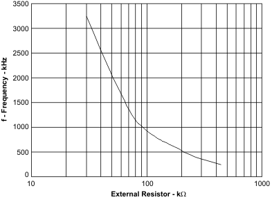 Figure 7. Switching Frequency vs External Resistor
Alternatively, the TPS61175-Q1 switching frequency will synchronize to an external clock signal that is applied to the SYNC pin. The logic level of the external clock is shown in the specification table. The duty cycle of the clock is recommended in the range of 10% to 90%. The resistor also must be connected to the FREQ pin when IC is switching by the external clock. The external clock frequency must be within ±20% of the corresponding frequency set by the resistor. For example, if the corresponding frequency as set by a resistor on the FREQ pin is 1.2-MHz, the external clock signal should be in the range of 0.96-MHz to 1.44-MHz.
If the external clock signal is higher than the frequency per the resistor on the FREQ pin, the maximum duty cycle specification (DMAX) should be lowered by 2%. For instance, if the resistor set value is 2.5MHz, and the external clock is 3MHz, DMAX is 87% instead of 89%.
8.3.2 Soft Start
The TPS61175-Q1 has a built-in soft start circuit which significantly reduces the start-up current spike and output voltage overshoot. When the IC is enabled, an internal bias current (6-μA typically) charges a capacitor (C3) on the SS pin. The voltage at the capacitor clamps the output of the internal error amplifier that determines the duty cycle of PWM control, thereby the input inrush current is eliminated. Once the capacitor reaches 1.8-V, the soft start cycle is completed and the soft start voltage no longer clamps the error amplifier output. Refer to Figure 7 for the soft start waveform. See Table 2 for C3 and corresponding soft start time. A 47-nF capacitor eliminates the output overshoot and reduces the peak inductor current for most applications.
Table 2. Soft Start Time vs C3
| VIN (V) | VOUT (V) | Load (A) | COUT (μF) | fSW (MHz) | C3 (nF) | tSS(ms) | Overshot (mV) |
|---|---|---|---|---|---|---|---|
| 5 | 24 | 0.4 | 10 | 1.2 | 47 | 4 | none |
| 10 | 0.8 | 210 | |||||
| 12 | 35 | 0.6 | 10 | 2 | 100 | 6.5 | none |
| 10 | 0.4 | 300 |
When the EN is pulled low for 10-ms, the IC enters shutdown and the SS capacitor discharges through a 5kΩ resistor for the next soft start.
8.3.3 Overcurrent Protection
The TPS61175-Q1 has a cycle-by-cycle overcurrent limit protection that turns off the power switch once the inductor current reaches the overcurrent limit threshold. The PWM circuitry resets itself at the beginning of the next switch cycle. During an overcurrent event, the output voltage begins to droop as a function of the load on the output. When the FB voltage drops lower than 0.9-V, the switching frequency is automatically reduced to 1/4 of the set value. The switching frequency does not reset until the overcurrent condition is removed. This feature is disabled during soft start.
8.3.4 Enable and Thermal Shutdown
The TPS61175-Q1 enters shutdown when the EN voltage is less than 0.4-V for more than 10-ms. In shutdown, the input supply current for the device is less than 1.5-μA (max). The EN pin has an internal 800-kΩ pull down resistor to disable the device when it is floating.
An internal thermal shutdown turns off the device when the typical junction temperature of 160°C is exceeded. The IC restarts when the junction temperature drops by 15°C.
8.3.5 Under Voltage Lockout (UVLO)
An under voltage lockout circuit prevents mis-operation of the device at input voltages below 2.5-V (typical). When the input voltage is below the under voltage threshold, the device remains off and the internal switch FET is turned off. The under voltage lockout threshold is set below minimum operating voltage of 2.9V to avoid any transient VIN dip triggering the UVLO and causing the device to reset. For the input voltages between UVLO threshold and 2.9V, the device attempts to operate, but the specifications are not ensured.
8.4 Device Functional Modes
8.4.1 Minimum on Time and Pulse Skipping
Once the PWM switch is turned on, the TPS61175-Q1 has minimum ON pulse width of 60-ns. This sets the limit of the minimum duty cycle of the PWM switch, and it is independent of the set switching frequency. When operating conditions result in the TPS61175-Q1 having a minimum ON pulse width less than 60-ns, the IC enters pulse-skipping mode. In this mode, the device keeps the power switch off for several switching cycles to keep the output voltage from rising above the regulated voltage. This operation typically occurs in light load condition when the PWM operates in discontinuous mode. Pulse skipping increases the output voltage ripple, see Figure 15.
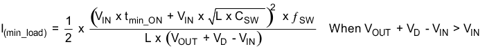
If the switching frequency is above 1.2 MHz, the pulse-skipping operation may not function. The TPS61175-Q1 will always run in PWM mode with minimum ON pulse width. To keep the output voltage in regulation, a minimum load is required. The minimum load is related to the input voltage, output voltage, switching frequency, external inductor value and the maximum value of the minimum ON pulse width. Use Equation 1 and Equation 2 to calculate the required minimum load at the worst case. The maximum tmin_ON could be estimated to 80 ns. CSW is the total parasite capacitance at the switching node SW pin. It could be estimated to 100 pF.