ZHCS026C December 2010 – February 2016 TPS57060-Q1
PRODUCTION DATA.
- 1 特征
- 2 应用
- 3 说明
- 4 修订历史记录
- 5 Pin Configuration and Functions
- 6 Specifications
-
7 Detailed Description
- 7.1 Overview
- 7.2 Functional Block Diagram
- 7.3
Feature Description
- 7.3.1 Fixed Frequency PWM Control
- 7.3.2 Slope Compensation Output Current
- 7.3.3 Low Dropout Operation and Bootstrap Voltage (BOOT)
- 7.3.4 Error Amplifier
- 7.3.5 Voltage Reference
- 7.3.6 Adjusting the Output Voltage
- 7.3.7 Enable and Adjusting Undervoltage Lockout (UVLO)
- 7.3.8 Slow Start and Tracking Pin (SS/TR)
- 7.3.9 Overload Recovery Circuit
- 7.3.10 Constant Switching Frequency and Timing Resistor (RT/CLK Pin)
- 7.3.11 Overcurrent Protection and Frequency Shift
- 7.3.12 Selecting the Switching Frequency
- 7.3.13 How to Interface to RT/CLK Pin
- 7.3.14 Power Good (PWRGD Pin)
- 7.3.15 Overvoltage Transient Protection
- 7.3.16 Thermal Shutdown
- 7.3.17 Small Signal Model for Loop Response
- 7.3.18 Simple Small-Signal Model for Peak Current-Mode Control
- 7.3.19 Small Signal Model for Frequency Compensation
- 7.4 Device Functional Modes
-
8 Application and Implementation
- 8.1 Application Information
- 8.2
Typical Application
- 8.2.1 Design Requirements
- 8.2.2
Detailed Design Procedure
- 8.2.2.1 Selecting the Switching Frequency
- 8.2.2.2 Output Inductor Selection (LO)
- 8.2.2.3 Output Capacitor
- 8.2.2.4 Catch Diode
- 8.2.2.5 Input Capacitor
- 8.2.2.6 Slow Start Capacitor
- 8.2.2.7 Bootstrap Capacitor Selection
- 8.2.2.8 Undervoltage Lockout Set Point
- 8.2.2.9 Output Voltage and Feedback Resistors Selection
- 8.2.2.10 Compensation
- 8.2.2.11 Discontinuous Mode and Eco Mode Boundary
- 8.2.3 Application Curves
- 9 Power Supply Recommendations
- 10Layout
- 11器件和文档支持
- 12机械、封装和可订购信息
封装选项
机械数据 (封装 | 引脚)
散热焊盘机械数据 (封装 | 引脚)
订购信息
7.4.2 Pulse Skip Eco-Mode
The TPS57060-Q1 device operates in a pulse-skip Eco mode at light load currents to improve efficiency by reducing switching and gate drive losses. The TPS57060-Q1 device is designed so that if the output voltage is within regulation and the peak switch current at the end of any switching cycle is below the pulse skipping current threshold, the device enters Eco mode. This current threshold is the current level corresponding to a nominal COMP voltage of 500 mV.
When in Eco-mode, the COMP pin voltage is clamped at 500 mV and the high-side MOSFET is inhibited. Further decreases in load current or in output voltage cannot drive the COMP pin below this clamp voltage level.
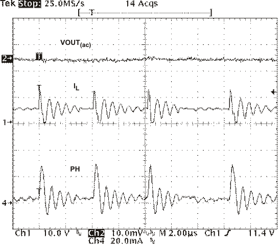
Because the device is not switching, the output voltage begins to decay. As the voltage control loop compensates for the falling output voltage, the COMP pin voltage begins to rise. At this time, the high-side MOSFET is enabled and a switching pulse initiates on the next switching cycle. The peak current is set by the COMP pin voltage. The output voltage re-charges the regulated value (see Figure 50), then the peak switch current starts to decrease, and eventually falls below the Eco mode threshold at which time the device again enters Eco mode.
For Eco mode operation, the TPS57060-Q1 device senses peak current, not average or load current, so the load current where the device enters Eco mode is dependent on the minimum on-time, input voltage, output voltage, and output inductance value. For example, the circuit in Figure 51 enters Eco mode at about 20 mA of output current. When the load current is low and the output voltage is within regulation, the device enters a sleep mode and draws only 116-μA input quiescent current. The internal PLL remains operating when in sleep mode. When operating at light load currents in the pulse skip mode, the switching transitions occur synchronously with the external clock signal.
 Figure 50. Pulse-Skip Mode Operation