ZHCS026C December 2010 – February 2016 TPS57060-Q1
PRODUCTION DATA.
- 1 特征
- 2 应用
- 3 说明
- 4 修订历史记录
- 5 Pin Configuration and Functions
- 6 Specifications
-
7 Detailed Description
- 7.1 Overview
- 7.2 Functional Block Diagram
- 7.3
Feature Description
- 7.3.1 Fixed Frequency PWM Control
- 7.3.2 Slope Compensation Output Current
- 7.3.3 Low Dropout Operation and Bootstrap Voltage (BOOT)
- 7.3.4 Error Amplifier
- 7.3.5 Voltage Reference
- 7.3.6 Adjusting the Output Voltage
- 7.3.7 Enable and Adjusting Undervoltage Lockout (UVLO)
- 7.3.8 Slow Start and Tracking Pin (SS/TR)
- 7.3.9 Overload Recovery Circuit
- 7.3.10 Constant Switching Frequency and Timing Resistor (RT/CLK Pin)
- 7.3.11 Overcurrent Protection and Frequency Shift
- 7.3.12 Selecting the Switching Frequency
- 7.3.13 How to Interface to RT/CLK Pin
- 7.3.14 Power Good (PWRGD Pin)
- 7.3.15 Overvoltage Transient Protection
- 7.3.16 Thermal Shutdown
- 7.3.17 Small Signal Model for Loop Response
- 7.3.18 Simple Small-Signal Model for Peak Current-Mode Control
- 7.3.19 Small Signal Model for Frequency Compensation
- 7.4 Device Functional Modes
-
8 Application and Implementation
- 8.1 Application Information
- 8.2
Typical Application
- 8.2.1 Design Requirements
- 8.2.2
Detailed Design Procedure
- 8.2.2.1 Selecting the Switching Frequency
- 8.2.2.2 Output Inductor Selection (LO)
- 8.2.2.3 Output Capacitor
- 8.2.2.4 Catch Diode
- 8.2.2.5 Input Capacitor
- 8.2.2.6 Slow Start Capacitor
- 8.2.2.7 Bootstrap Capacitor Selection
- 8.2.2.8 Undervoltage Lockout Set Point
- 8.2.2.9 Output Voltage and Feedback Resistors Selection
- 8.2.2.10 Compensation
- 8.2.2.11 Discontinuous Mode and Eco Mode Boundary
- 8.2.3 Application Curves
- 9 Power Supply Recommendations
- 10Layout
- 11器件和文档支持
- 12机械、封装和可订购信息
封装选项
机械数据 (封装 | 引脚)
散热焊盘机械数据 (封装 | 引脚)
订购信息
6.6 Typical Characteristics
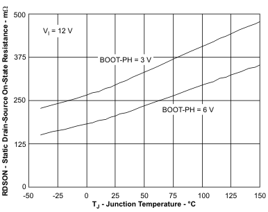
Figure 1. On Resistance vs Junction Temperature
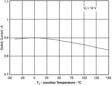
Figure 3. Switch Current Limit vs Junction Temperature
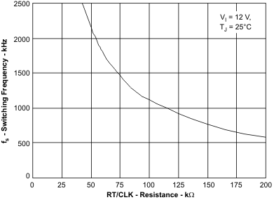
Figure 5. Switching Frequency vs RT/CLK Resistance High-Frequency Range
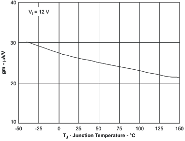
Figure 7. EA Transconductance During Slow Start vs Junction Temperature
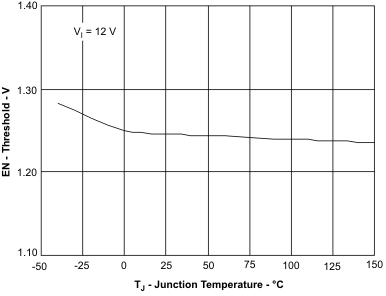
Figure 9. EN Pin Voltage vs Junction Temperature
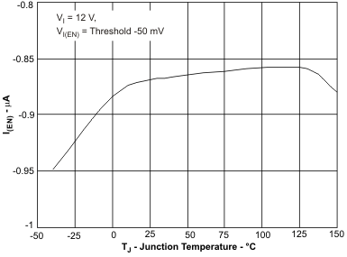
Figure 11. EN Pin Current vs Junction Temperature
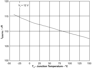
Figure 13. SS/TR Discharge Current vs Junction Temperature
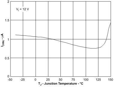
Figure 15. Shutdown Supply Current vs Junction Temperature
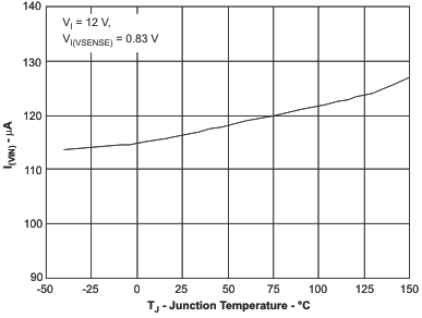
Figure 17. VIN Supply Current vs Junction Temperature
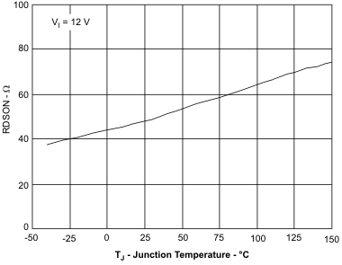
Figure 19. PWRGD On Resistance vs Junction Temperature
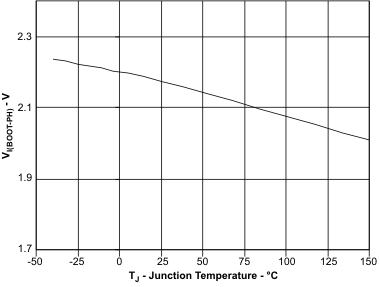
Figure 21. BOOT-PH UVLO vs Junction Temperature
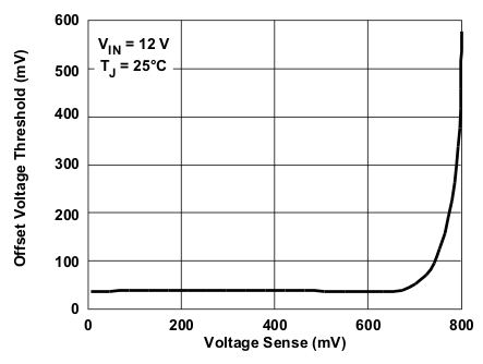
Figure 23. SS/TR to VSENSE Offset vs VSENSE
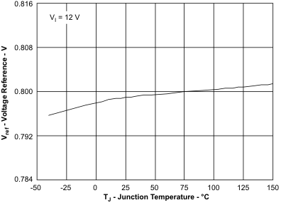
Figure 2. Voltage Reference vs Junction Temperature
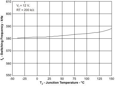
Figure 4. Switching Frequency vs Junction Temperature
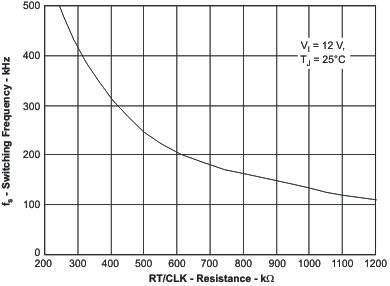
Figure 6. Switching Frequency vs RT/CLK Resistance Low-Frequency Range
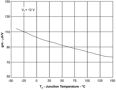
Figure 8. EA Transconductance vs Junction Temperature
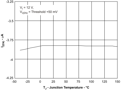
Figure 10. EN Pin Current vs Junction Temperature
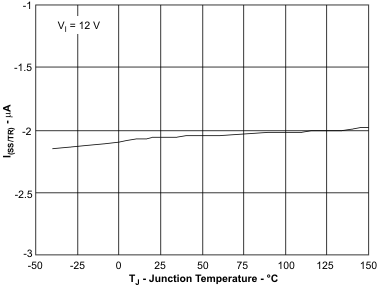
Figure 12. SS/TR Charge Current vs Junction Temperature
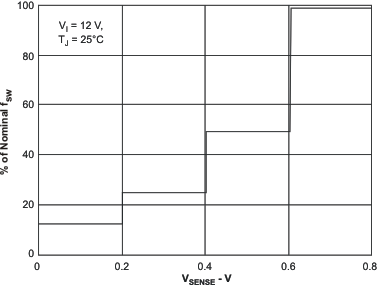
Figure 14. Switching Frequency vs VSENSE
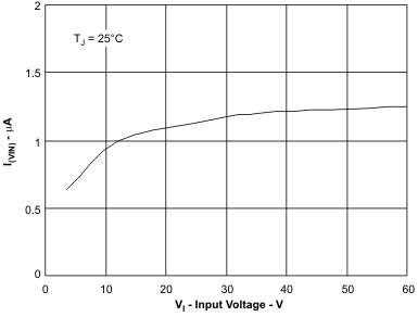
Figure 16. Shutdown Supply Current vs Input Voltage (VIN)
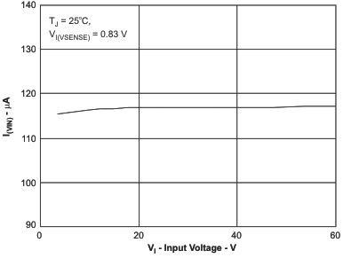
Figure 18. VIN Supply Current vs Input Voltage
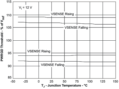
Figure 20. PWRGD Threshold vs Junction Temperature
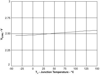
Figure 22. Input Voltage (UVLO) vs Junction Temperature
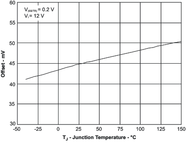
Figure 24. SS/TR to VSENSE Offset vs Temperature