ZHCSNA2 October   2021 TPS563212

PRODUCTION DATA  

  1. 特性
  2. 应用
  3. 说明
  4. Revision History
  5. Pin Configuration and Functions
  6. Specifications
    1. 6.1 Absolute Maximum Ratings
    2. 6.2 ESD Ratings
    3. 6.3 Recommended Operating Conditions
    4. 6.4 Thermal Information
    5. 6.5 Electrical Characteristics
    6. 6.6 Typical Characteristics
  7. Detailed Description
    1. 7.1 Overview
    2. 7.2 Functional Block Diagram
    3. 7.3 Feature Description
      1. 7.3.1 Advanced Emulated Current Mode Control
      2. 7.3.2 Mode Selection and PG/SS Pin Function Configuration
      3. 7.3.3 Power Good (PG)
      4. 7.3.4 Soft Start and Pre-Biased Soft Start
      5. 7.3.5 Output Discharge Through PG/SS Pin
      6. 7.3.6 Precise Enable and Adjusting Undervoltage Lockout
      7. 7.3.7 Overcurrent Limit and Undervoltage Protection
      8. 7.3.8 Overvoltage Protection
      9. 7.3.9 Thermal Shutdown
    4. 7.4 Device Functional Modes
      1. 7.4.1 Shutdown Mode
      2. 7.4.2 Active Mode
      3. 7.4.3 FCCM Operation
      4. 7.4.4 CCM Operation
      5. 7.4.5 DCM Operation and Eco-mode Operation
      6. 7.4.6 On-Time Extension for Large Duty Cycle Operation
  8. Application and Implementation
    1. 8.1 Application Information
    2. 8.2 Typical Application
      1. 8.2.1 Design Requirements
      2. 8.2.2 Detailed Design Procedure
        1. 8.2.2.1 Custom Design With WEBENCH® Tools
        2. 8.2.2.2 Output Voltage Resistors Selection
        3. 8.2.2.3 Output Inductor Selection
        4. 8.2.2.4 Output Capacitor Selection
        5. 8.2.2.5 Input Capacitor Selection
        6. 8.2.2.6 Bootstrap Capacitor Selection
        7. 8.2.2.7 Undervoltage Lockout Set Point
      3. 8.2.3 Application Curves
  9. Power Supply Recommendations
  10. 10Layout
    1. 10.1 Layout Guidelines
    2. 10.2 Layout Example
  11. 11Device and Documentation Support
    1. 11.1 Device Support
      1. 11.1.1 第三方产品免责声明
      2. 11.1.2 Development Support
        1. 11.1.2.1 Custom Design With WEBENCH® Tools
    2. 11.2 接收文档更新通知
    3. 11.3 支持资源
    4. 11.4 Trademarks
    5. 11.5 Electrostatic Discharge Caution
    6. 11.6 术语表
  12. 12Mechanical, Packaging, and Orderable Information

封装选项

机械数据 (封装 | 引脚)
散热焊盘机械数据 (封装 | 引脚)
订购信息

Output Voltage Resistors Selection

The output voltage is set with a resistor divider from the output node to the FB pin. TI recommends using 1% tolerance or better divider resistors. Referring to the application schematic of Figure 8-1, start with 10 kΩ or 20 kΩ for R9 and use Equation 11 to calculate R8. To improve efficiency at light loads, consider using larger value resistors. If the values are too high, the regulator is more susceptible to noise and voltage errors from the FB input current are noticeable.

Equation 11. GUID-3C0703EF-8A66-4B96-9A02-EBBD8863DAF8-low.gif

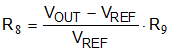
Table 8-2 shows the recommended components value for common output voltages.