ZHCSNA2 October 2021 TPS563212
PRODUCTION DATA
- 1 特性
- 2 应用
- 3 说明
- 4 Revision History
- 5 Pin Configuration and Functions
- 6 Specifications
-
7 Detailed Description
- 7.1 Overview
- 7.2 Functional Block Diagram
- 7.3
Feature Description
- 7.3.1 Advanced Emulated Current Mode Control
- 7.3.2 Mode Selection and PG/SS Pin Function Configuration
- 7.3.3 Power Good (PG)
- 7.3.4 Soft Start and Pre-Biased Soft Start
- 7.3.5 Output Discharge Through PG/SS Pin
- 7.3.6 Precise Enable and Adjusting Undervoltage Lockout
- 7.3.7 Overcurrent Limit and Undervoltage Protection
- 7.3.8 Overvoltage Protection
- 7.3.9 Thermal Shutdown
- 7.4 Device Functional Modes
- 8 Application and Implementation
- 9 Power Supply Recommendations
- 10Layout
- 11Device and Documentation Support
- 12Mechanical, Packaging, and Orderable Information
7.3.2 Mode Selection and PG/SS Pin Function Configuration
The device requires a mode resistor to select the operations mode under light load and configure the function of pin 1. Table 7-1 shows the MODE pin settings.
| MODE RESISTOR RANGE | RECOMMENDED MODE RESISTOR VALUE | OPERATION MODE IN LIGHT LOAD | FUNCTION OF PG/SS PIN |
|---|---|---|---|
| [0, 12] kΩ | 0 | Eco-mode | Power Good |
| [30, 50] kΩ | 47 kΩ | Eco-mode | Soft Start |
| [83, 120] kΩ | 100 kΩ | FCCM | Soft Start |
| [180, ∞] kΩ | Float | FCCM | Power Good |
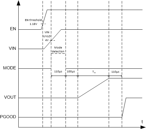
Figure 7-1 shows the typical start-up sequence of the device once the enable signal triggers the EN turn-on threshold. After the voltage of VIN crosses the UVLO rising threshold, it takes approximately 110 μs to finish reading and setting of the MODE pin. After this process, the MODE status is latched and does not change until VIN or EN toggles to restart this device. Then, the soft-start function begins to ramp up the reference voltage to the PWM comparator.
 Figure 7-1 Power-Up Sequence