ZHCSNA2 October   2021 TPS563212

PRODUCTION DATA  

  1. 特性
  2. 应用
  3. 说明
  4. Revision History
  5. Pin Configuration and Functions
  6. Specifications
    1. 6.1 Absolute Maximum Ratings
    2. 6.2 ESD Ratings
    3. 6.3 Recommended Operating Conditions
    4. 6.4 Thermal Information
    5. 6.5 Electrical Characteristics
    6. 6.6 Typical Characteristics
  7. Detailed Description
    1. 7.1 Overview
    2. 7.2 Functional Block Diagram
    3. 7.3 Feature Description
      1. 7.3.1 Advanced Emulated Current Mode Control
      2. 7.3.2 Mode Selection and PG/SS Pin Function Configuration
      3. 7.3.3 Power Good (PG)
      4. 7.3.4 Soft Start and Pre-Biased Soft Start
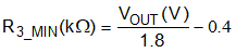
      5. 7.3.5 Output Discharge Through PG/SS Pin
      6. 7.3.6 Precise Enable and Adjusting Undervoltage Lockout
      7. 7.3.7 Overcurrent Limit and Undervoltage Protection
      8. 7.3.8 Overvoltage Protection
      9. 7.3.9 Thermal Shutdown
    4. 7.4 Device Functional Modes
      1. 7.4.1 Shutdown Mode
      2. 7.4.2 Active Mode
      3. 7.4.3 FCCM Operation
      4. 7.4.4 CCM Operation
      5. 7.4.5 DCM Operation and Eco-mode Operation
      6. 7.4.6 On-Time Extension for Large Duty Cycle Operation
  8. Application and Implementation
    1. 8.1 Application Information
    2. 8.2 Typical Application
      1. 8.2.1 Design Requirements
      2. 8.2.2 Detailed Design Procedure
        1. 8.2.2.1 Custom Design With WEBENCH® Tools
        2. 8.2.2.2 Output Voltage Resistors Selection
        3. 8.2.2.3 Output Inductor Selection
        4. 8.2.2.4 Output Capacitor Selection
        5. 8.2.2.5 Input Capacitor Selection
        6. 8.2.2.6 Bootstrap Capacitor Selection
        7. 8.2.2.7 Undervoltage Lockout Set Point
      3. 8.2.3 Application Curves
  9. Power Supply Recommendations
  10. 10Layout
    1. 10.1 Layout Guidelines
    2. 10.2 Layout Example
  11. 11Device and Documentation Support
    1. 11.1 Device Support
      1. 11.1.1 第三方产品免责声明
      2. 11.1.2 Development Support
        1. 11.1.2.1 Custom Design With WEBENCH® Tools
    2. 11.2 接收文档更新通知
    3. 11.3 支持资源
    4. 11.4 Trademarks
    5. 11.5 Electrostatic Discharge Caution
    6. 11.6 术语表
  12. 12Mechanical, Packaging, and Orderable Information

封装选项

机械数据 (封装 | 引脚)
散热焊盘机械数据 (封装 | 引脚)
订购信息

Output Discharge Through PG/SS Pin

If the PG function is selected, the device pulls the PG/SS pin low when the device is shut down by one of the following:

  • EN
  • OVP
  • UVP
  • UVLO
  • Thermal shutdown

In those cases, the user can connect PG/SS to VOUT through a resistor to discharge VOUT (see Figure 7-2). The discharge rate can be adjusted by R3, which is also used to pull up the PG/SS pin in normal operation. The minimum supply voltage required for the discharge function to remain active is typically 2.5 V. For reliability, keep the maximum current into the PG/SS pin less than 1.8 mA. Given an output voltage, the minimum resistance of R3 can be calculated in Equation 11.

Equation 2. GUID-867E3CBE-394D-4A41-BBEE-7B731E74A7B6-low.gif
Figure 7-2 Discharge VOUT Through PG/SS Pin with the TPS563212