ZHCS137F March 2011 – October 2017 TPS54622
PRODUCTION DATA.
- 1 特性
- 2 应用
- 3 说明
- 4 修订历史记录
- 5 Pin Configurations and Functions
- 6 Specifications
-
7 Detailed Description
- 7.1 Overview
- 7.2 Functional Block Diagram
- 7.3
Feature Description
- 7.3.1 Fixed-Frequency PWM Control
- 7.3.2 Continuous Current Mode Operation (CCM)
- 7.3.3 VIN and Power VIN Pins (VIN and PVIN)
- 7.3.4 Voltage Reference
- 7.3.5 Adjusting the Output Voltage
- 7.3.6 Safe Start-Up Into Prebiased Outputs
- 7.3.7 Error Amplifier
- 7.3.8 Slope Compensation
- 7.3.9 Enable and Adjusting Undervoltage Lockout
- 7.3.10 Adjustable Switching Frequency and Synchronization (RT/CLK)
- 7.3.11 Slow Start (SS/TR)
- 7.3.12 Power Good (PWRGD)
- 7.3.13 Output Overvoltage Protection (OVP)
- 7.3.14 Overcurrent Protection
- 7.3.15 Thermal Shutdown
- 7.3.16 Small Signal Model for Loop Response
- 7.3.17 Simple Small Signal Model for Peak Current Mode Control
- 7.3.18 Small Signal Model for Frequency Compensation
- 7.4 Device Functional Modes
-
8 Application and Implementation
- 8.1 Application Information
- 8.2
Typical Application
- 8.2.1 Design Requirements
- 8.2.2
Detailed Design Procedures
- 8.2.2.1 Custom Design With WEBENCH® Tools
- 8.2.2.2 Operating Frequency
- 8.2.2.3 Output Inductor Selection
- 8.2.2.4 Output Capacitor Selection
- 8.2.2.5 Input Capacitor Selection
- 8.2.2.6 Slow-Start Capacitor Selection
- 8.2.2.7 Bootstrap Capacitor Selection
- 8.2.2.8 Undervoltage Lockout Setpoint
- 8.2.2.9 Output Voltage Feedback Resistor Selection
- 8.2.2.10 Compensation Component Selection
- 8.2.2.11 Fast Transient Considerations
- 8.2.3 Application Curves
- 9 Power Supply Recommendations
- 10Layout
- 11器件和文档支持
- 12机械、封装和可订购信息
7.4.2 Synchronization (CLK Mode)
An internal phase locked loop (PLL) has been implemented to allow synchronization from 200 kHz to 1600 kHz, and to easily switch from RT mode to CLK mode.
To implement the synchronization feature, connect a square wave clock signal to the RT/CLK pin with a duty cycle from 20% to 80%. The clock signal amplitude must transition lower than 0.8 V and higher than 2 V. The start of the switching cycle is synchronized to the falling edge of RT/CLK pin.
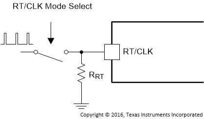
In applications where both RT mode and CLK mode are needed, the device can be configured as shown in Figure 25. Before the external clock is present, the device works in RT mode and the switching frequency is set by RT resistor. When the external clock is present, the CLK mode overrides the RT mode. The first time the SYNC pin is pulled above the RT/CLK high threshold (2 V), the device switches from the RT mode to the CLK mode and the RT/CLK pin becomes high impedance as the PLL starts to lock onto the frequency of the external clock. TI does not recommended switching from the CLK mode back to the RT mode because the internal switching frequency drops to 100 kHz first before returning to the switching frequency set by RT resistor.
 Figure 25. Works With Both RT Mode and CLK Mode