ZHCS137F March 2011 – October 2017 TPS54622
PRODUCTION DATA.
- 1 特性
- 2 应用
- 3 说明
- 4 修订历史记录
- 5 Pin Configurations and Functions
- 6 Specifications
-
7 Detailed Description
- 7.1 Overview
- 7.2 Functional Block Diagram
- 7.3
Feature Description
- 7.3.1 Fixed-Frequency PWM Control
- 7.3.2 Continuous Current Mode Operation (CCM)
- 7.3.3 VIN and Power VIN Pins (VIN and PVIN)
- 7.3.4 Voltage Reference
- 7.3.5 Adjusting the Output Voltage
- 7.3.6 Safe Start-Up Into Prebiased Outputs
- 7.3.7 Error Amplifier
- 7.3.8 Slope Compensation
- 7.3.9 Enable and Adjusting Undervoltage Lockout
- 7.3.10 Adjustable Switching Frequency and Synchronization (RT/CLK)
- 7.3.11 Slow Start (SS/TR)
- 7.3.12 Power Good (PWRGD)
- 7.3.13 Output Overvoltage Protection (OVP)
- 7.3.14 Overcurrent Protection
- 7.3.15 Thermal Shutdown
- 7.3.16 Small Signal Model for Loop Response
- 7.3.17 Simple Small Signal Model for Peak Current Mode Control
- 7.3.18 Small Signal Model for Frequency Compensation
- 7.4 Device Functional Modes
-
8 Application and Implementation
- 8.1 Application Information
- 8.2
Typical Application
- 8.2.1 Design Requirements
- 8.2.2
Detailed Design Procedures
- 8.2.2.1 Custom Design With WEBENCH® Tools
- 8.2.2.2 Operating Frequency
- 8.2.2.3 Output Inductor Selection
- 8.2.2.4 Output Capacitor Selection
- 8.2.2.5 Input Capacitor Selection
- 8.2.2.6 Slow-Start Capacitor Selection
- 8.2.2.7 Bootstrap Capacitor Selection
- 8.2.2.8 Undervoltage Lockout Setpoint
- 8.2.2.9 Output Voltage Feedback Resistor Selection
- 8.2.2.10 Compensation Component Selection
- 8.2.2.11 Fast Transient Considerations
- 8.2.3 Application Curves
- 9 Power Supply Recommendations
- 10Layout
- 11器件和文档支持
- 12机械、封装和可订购信息
6.6 Typical Characteristics
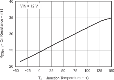
Figure 1. High-Side RDS(on) vs Temperature
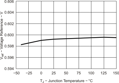
Figure 3. Voltage Reference vs Temperature
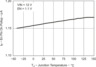
Figure 7. Pin Pullup Current vs Temperature
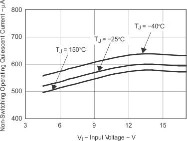
Figure 9. Non-Switching Operating Quiescent Current (VIN) vs Input Voltage
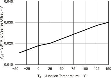
Figure 11. (SS/TR - VSENSE) Offset vs Temperature
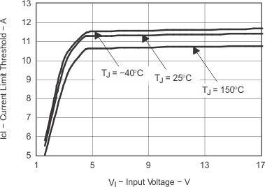
Figure 13. High-Side Current Limit Threshold vs Input Voltage
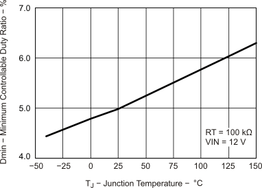
Figure 15. Minimum Controllable Duty Ratio vs Junction Temperature
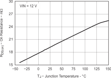
Figure 2. Low-Side RDS(on) vs Temperature
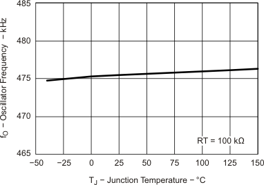
Figure 4. Oscillator Frequency vs Temperature
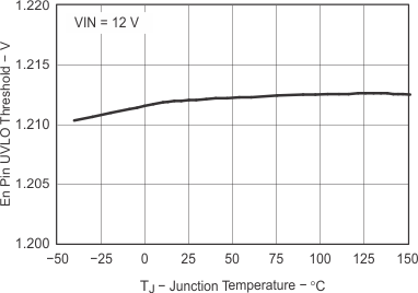
Figure 8. Pin UVLO Threshold vs Temperature
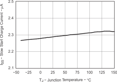
Figure 10. Slow Start Charge Current vs Temperature
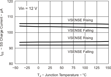
Figure 12. PWRGD Threshold vs Temperature
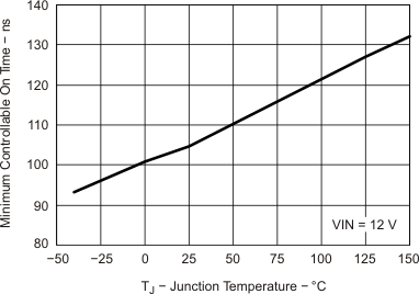
Figure 14. Minimum Controllable On-Time vs Temperature
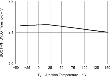
Figure 16. BOOT-PH UVLO Threshold vs Temperature
