ZHCSF14D March 2010 – October 2018 TPS54260
PRODUCTION DATA.
- 1 特性
- 2 应用
- 3 说明
- 4 修订历史记录
- 5 Pin Configuration and Functions
- 6 Specifications
-
7 Detailed Description
- 7.1 Overview
- 7.2 Functional Block Diagram
- 7.3
Feature Description
- 7.3.1 Fixed Frequency PWM Control
- 7.3.2 Slope Compensation Output Current
- 7.3.3 Pulse-Skip Eco-Mode
- 7.3.4 Low-Dropout Operation and Bootstrap Voltage (BOOT)
- 7.3.5 Error Amplifier
- 7.3.6 Voltage Reference
- 7.3.7 Adjusting the Output Voltage
- 7.3.8 Enable and Adjusting Undervoltage Lockout
- 7.3.9 Slow-Start / Tracking Pin (SS/TR)
- 7.3.10 Overload Recovery Circuit
- 7.3.11 Sequencing
- 7.3.12 Constant Switching Frequency and Timing Resistor (RT/CLK Pin)
- 7.3.13 Overcurrent Protection and Frequency Shift
- 7.3.14 Selecting the Switching Frequency
- 7.3.15 How to Interface to RT/CLK Pin
- 7.3.16 Powergood (PWRGD Pin)
- 7.3.17 Overvoltage Transient Protection
- 7.3.18 Thermal Shutdown
- 7.3.19 Small Signal Model for Loop Response
- 7.3.20 Simple Small Signal Model for Peak Current Mode Control
- 7.3.21 Small Signal Model for Frequency Compensation
- 7.4 Device Functional Modes
-
8 Application and Implementation
- 8.1 Application Information
- 8.2
Typical Applications
- 8.2.1
3.3-V Output Application
- 8.2.1.1 Design Requirements
- 8.2.1.2
Detailed Design Procedure
- 8.2.1.2.1 Custom Design With WEBENCH® Tools
- 8.2.1.2.2 Selecting the Switching Frequency
- 8.2.1.2.3 Output Inductor Selection (LO)
- 8.2.1.2.4 Output Capacitor
- 8.2.1.2.5 Catch Diode
- 8.2.1.2.6 Input Capacitor
- 8.2.1.2.7 Slow-Start Capacitor
- 8.2.1.2.8 Bootstrap Capacitor Selection
- 8.2.1.2.9 Undervoltage Lock Out Set Point
- 8.2.1.2.10 Output Voltage and Feedback Resistors Selection
- 8.2.1.2.11 Compensation
- 8.2.1.2.12 Discontinuous Mode and Eco-Mode Boundary
- 8.2.1.2.13 Power Dissipation Estimate
- 8.2.1.3 Application Curves
- 8.2.2 Inverting Power Supply
- 8.2.3 Split-Rail Power Supply
- 8.2.4 12-V to 3.8-V GSM Power Supply
- 8.2.5 24-V to 4.2-V GSM Power Supply
- 8.2.1
3.3-V Output Application
- 9 Power Supply Recommendations
- 10Layout
- 11器件和文档支持
- 12机械、封装和可订购信息
封装选项
机械数据 (封装 | 引脚)
散热焊盘机械数据 (封装 | 引脚)
订购信息
7.3.21 Small Signal Model for Frequency Compensation
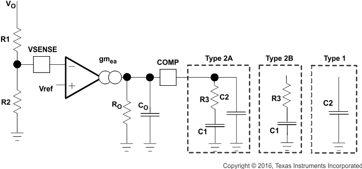
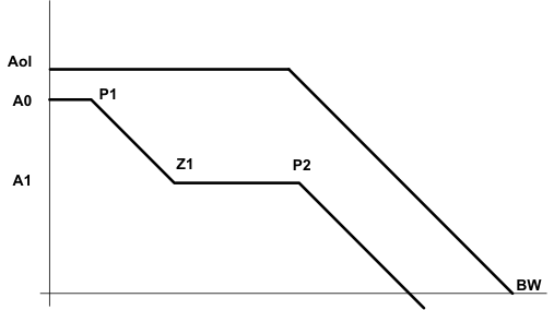
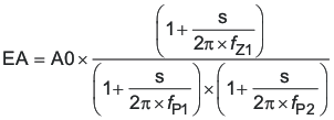
The TPS54260 uses a transconductance amplifier for the error amplifier and readily supports three of the commonly-used frequency compensation circuits. Compensation circuits Type 2A, Type 2B, and Type 1 are shown in Figure 48. Type 2 circuits most likely implemented in high-bandwidth power-supply designs using low-ESR output capacitors. The Type 1 circuit is used with power-supply designs with high-ESR aluminum electrolytic or tantalum capacitors.. Equation 18 and Equation 19 show how to relate the frequency response of the amplifier to the small signal model in Figure 48. The open-loop gain and bandwidth are modeled using the RO and CO shown in Figure 48. See the application section for a design example using a Type 2A network with a low-ESR output capacitor.
Equation 18 through Equation 27 are provided as a reference for those who prefer to compensate using the preferred methods. Those who prefer to use prescribed method use the method outlined in the application section or use switched information.
 Figure 48. Types of Frequency Compensation
  Figure 49. Frequency Response of the Type 2A and Type 2B Frequency Compensation


