ZHCSF14D March 2010 – October 2018 TPS54260
PRODUCTION DATA.
- 1 特性
- 2 应用
- 3 说明
- 4 修订历史记录
- 5 Pin Configuration and Functions
- 6 Specifications
-
7 Detailed Description
- 7.1 Overview
- 7.2 Functional Block Diagram
- 7.3
Feature Description
- 7.3.1 Fixed Frequency PWM Control
- 7.3.2 Slope Compensation Output Current
- 7.3.3 Pulse-Skip Eco-Mode
- 7.3.4 Low-Dropout Operation and Bootstrap Voltage (BOOT)
- 7.3.5 Error Amplifier
- 7.3.6 Voltage Reference
- 7.3.7 Adjusting the Output Voltage
- 7.3.8 Enable and Adjusting Undervoltage Lockout
- 7.3.9 Slow-Start / Tracking Pin (SS/TR)
- 7.3.10 Overload Recovery Circuit
- 7.3.11 Sequencing
- 7.3.12 Constant Switching Frequency and Timing Resistor (RT/CLK Pin)
- 7.3.13 Overcurrent Protection and Frequency Shift
- 7.3.14 Selecting the Switching Frequency
- 7.3.15 How to Interface to RT/CLK Pin
- 7.3.16 Powergood (PWRGD Pin)
- 7.3.17 Overvoltage Transient Protection
- 7.3.18 Thermal Shutdown
- 7.3.19 Small Signal Model for Loop Response
- 7.3.20 Simple Small Signal Model for Peak Current Mode Control
- 7.3.21 Small Signal Model for Frequency Compensation
- 7.4 Device Functional Modes
-
8 Application and Implementation
- 8.1 Application Information
- 8.2
Typical Applications
- 8.2.1
3.3-V Output Application
- 8.2.1.1 Design Requirements
- 8.2.1.2
Detailed Design Procedure
- 8.2.1.2.1 Custom Design With WEBENCH® Tools
- 8.2.1.2.2 Selecting the Switching Frequency
- 8.2.1.2.3 Output Inductor Selection (LO)
- 8.2.1.2.4 Output Capacitor
- 8.2.1.2.5 Catch Diode
- 8.2.1.2.6 Input Capacitor
- 8.2.1.2.7 Slow-Start Capacitor
- 8.2.1.2.8 Bootstrap Capacitor Selection
- 8.2.1.2.9 Undervoltage Lock Out Set Point
- 8.2.1.2.10 Output Voltage and Feedback Resistors Selection
- 8.2.1.2.11 Compensation
- 8.2.1.2.12 Discontinuous Mode and Eco-Mode Boundary
- 8.2.1.2.13 Power Dissipation Estimate
- 8.2.1.3 Application Curves
- 8.2.2 Inverting Power Supply
- 8.2.3 Split-Rail Power Supply
- 8.2.4 12-V to 3.8-V GSM Power Supply
- 8.2.5 24-V to 4.2-V GSM Power Supply
- 8.2.1
3.3-V Output Application
- 9 Power Supply Recommendations
- 10Layout
- 11器件和文档支持
- 12机械、封装和可订购信息
封装选项
机械数据 (封装 | 引脚)
散热焊盘机械数据 (封装 | 引脚)
订购信息
7.3.15 How to Interface to RT/CLK Pin
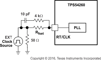
The RT/CLK pin can be used to synchronize the regulator to an external system clock. To implement the synchronization feature connect a square wave to the RT/CLK pin through the circuit network shown in Figure 42. The square wave amplitude must transition lower than 0.5 V and higher than 2.2 V on the RT/CLK pin and have an on time greater than 40 ns and an off-time greater than 40 ns. The synchronization frequency range is 300 kHz to 2200 kHz. The rising edge of the PH will be synchronized to the falling edge of RT/CLK pin signal. The external synchronization circuit should be designed in such a way that the device will have the default frequency set resistor connected from the RT/CLK pin to ground should the synchronization signal turn off. It is recommended to use a frequency set resistor connected as shown in Figure 42 through a 50-Ω resistor-to-ground. The resistor should set the switching frequency close to the external CLK frequency. TI recommends to AC couple the synchronization signal through a 10-pF ceramic capacitor to RT/CLK pin and a 4-kΩ series resistor. The series resistor reduces PH jitter in heavy-load applications when synchronizing to an external clock and in applications which transition from synchronizing to RT mode. The first time the CLK is pulled above the CLK threshold the device switches from the RT resistor frequency to PLL mode. The internal 0.5-V voltage source is removed and the CLK pin becomes high impedance as the PLL starts to lock onto the external signal. Since there is a PLL on the regulator the switching frequency can be higher or lower than the frequency set with the external resistor. The device transitions from the resistor mode to the PLL mode and then will increase or decrease the switching frequency until the PLL locks onto the CLK frequency within 100 µs.
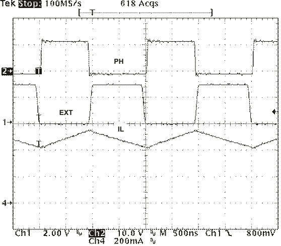
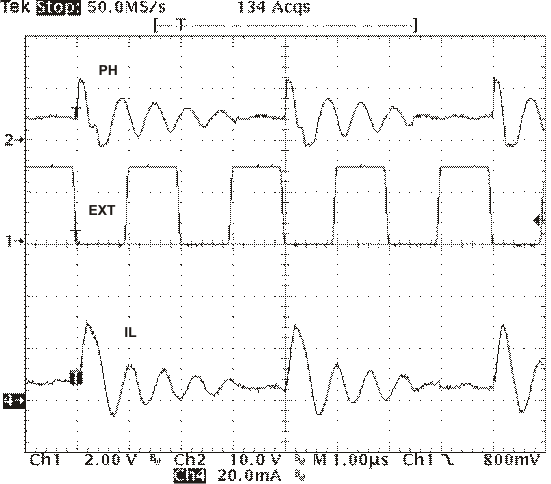
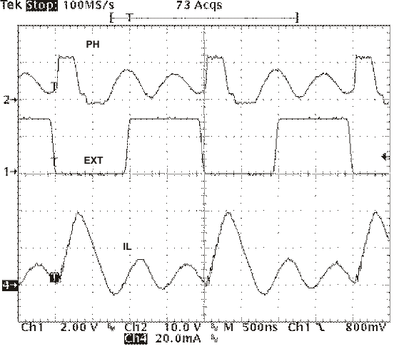
When the device transitions from the PLL to resistor mode the switching frequency will slow down from the CLK frequency to 150 kHz, then reapply the 0.5-V voltage and the resistor will then set the switching frequency. The switching frequency is divided by 8, 4, 2, and 1 as the voltage ramps from 0 to 0.8 V on VSENSE pin. The device implements a digital frequency shift to enable synchronizing to an external clock during normal start-up and fault conditions. Figure 43, Figure 44, and Figure 45 show the device synchronized to an external system clock in continuous conduction mode (CCM) discontinuous conduction (DCM) and pulse-skip mode (PSM).
 Figure 43. Plot of Synchronizing in CCM
  Figure 45. Plot of Synchronizing in PSM
  Figure 44. Plot of Synchronizing in DCM