ZHCSF14D March 2010 – October 2018 TPS54260
PRODUCTION DATA.
- 1 特性
- 2 应用
- 3 说明
- 4 修订历史记录
- 5 Pin Configuration and Functions
- 6 Specifications
-
7 Detailed Description
- 7.1 Overview
- 7.2 Functional Block Diagram
- 7.3
Feature Description
- 7.3.1 Fixed Frequency PWM Control
- 7.3.2 Slope Compensation Output Current
- 7.3.3 Pulse-Skip Eco-Mode
- 7.3.4 Low-Dropout Operation and Bootstrap Voltage (BOOT)
- 7.3.5 Error Amplifier
- 7.3.6 Voltage Reference
- 7.3.7 Adjusting the Output Voltage
- 7.3.8 Enable and Adjusting Undervoltage Lockout
- 7.3.9 Slow-Start / Tracking Pin (SS/TR)
- 7.3.10 Overload Recovery Circuit
- 7.3.11 Sequencing
- 7.3.12 Constant Switching Frequency and Timing Resistor (RT/CLK Pin)
- 7.3.13 Overcurrent Protection and Frequency Shift
- 7.3.14 Selecting the Switching Frequency
- 7.3.15 How to Interface to RT/CLK Pin
- 7.3.16 Powergood (PWRGD Pin)
- 7.3.17 Overvoltage Transient Protection
- 7.3.18 Thermal Shutdown
- 7.3.19 Small Signal Model for Loop Response
- 7.3.20 Simple Small Signal Model for Peak Current Mode Control
- 7.3.21 Small Signal Model for Frequency Compensation
- 7.4 Device Functional Modes
-
8 Application and Implementation
- 8.1 Application Information
- 8.2
Typical Applications
- 8.2.1
3.3-V Output Application
- 8.2.1.1 Design Requirements
- 8.2.1.2
Detailed Design Procedure
- 8.2.1.2.1 Custom Design With WEBENCH® Tools
- 8.2.1.2.2 Selecting the Switching Frequency
- 8.2.1.2.3 Output Inductor Selection (LO)
- 8.2.1.2.4 Output Capacitor
- 8.2.1.2.5 Catch Diode
- 8.2.1.2.6 Input Capacitor
- 8.2.1.2.7 Slow-Start Capacitor
- 8.2.1.2.8 Bootstrap Capacitor Selection
- 8.2.1.2.9 Undervoltage Lock Out Set Point
- 8.2.1.2.10 Output Voltage and Feedback Resistors Selection
- 8.2.1.2.11 Compensation
- 8.2.1.2.12 Discontinuous Mode and Eco-Mode Boundary
- 8.2.1.2.13 Power Dissipation Estimate
- 8.2.1.3 Application Curves
- 8.2.2 Inverting Power Supply
- 8.2.3 Split-Rail Power Supply
- 8.2.4 12-V to 3.8-V GSM Power Supply
- 8.2.5 24-V to 4.2-V GSM Power Supply
- 8.2.1
3.3-V Output Application
- 9 Power Supply Recommendations
- 10Layout
- 11器件和文档支持
- 12机械、封装和可订购信息
封装选项
机械数据 (封装 | 引脚)
散热焊盘机械数据 (封装 | 引脚)
订购信息
7.3.4 Low-Dropout Operation and Bootstrap Voltage (BOOT)
The TPS54260 has an integrated boot regulator, and requires a small ceramic capacitor between the BOOT and PH pins to provide the gate drive voltage for the high-side MOSFET. The BOOT capacitor is refreshed when the high-side MOSFET is off and the low-side diode conducts. The value of this ceramic capacitor should be 0.1 μF. A ceramic capacitor with an X7R or X5R grade dielectric with a voltage rating of 10 V or higher is recommended because of the stable characteristics overtemperature and voltage.
To improve dropout, the TPS54260 is designed to operate at 100% duty cycle as long as the BOOT to PH pin voltage is greater than 2.1 V. When the voltage from BOOT to PH drops below 2.1 V, the high-side MOSFET is turned off using an UVLO circuit which allows the low-side diode to conduct and refresh the charge on the BOOT capacitor. Since the supply current sourced from the BOOT capacitor is low, the high-side MOSFET can remain on for more switching cycles than are required to refresh the capacitor, thus the effective duty cycle of the switching regulator is high.
The effective duty cycle during dropout of the regulator is mainly influenced by the voltage drops across the power MOSFET, inductor resistance, low-side diode and printed circuit board resistance. During operating conditions in which the input voltage drops and the regulator is operating in continuous conduction mode, the high-side MOSFET can remain on for 100% of the duty cycle to maintain output regulation, until the BOOT to PH voltage falls below 2.1 V.
Pay attention in maximum duty cycle applications which experience extended time periods with light loads or no load. When the voltage across the BOOT capacitor falls below the 2.1V UVLO threshold, the high-side MOSFET is turned off, but there may not be enough inductor current to pull the PH pin down to recharge the BOOT capacitor. The high-side MOSFET of the regulator stops switching because the voltage across the BOOT capacitor is less than 2.1 V. The output capacitor then decays until the difference in the input voltage and output voltage is greater than 2.1 V, at which point the BOOT UVLO threshold is exceeded, and the device starts switching again until the desired output voltage is reached. This operating condition persists until the input voltage and/or the load current increases. TI recommends adjusting the VIN stop voltage greater than the BOOT UVLO trigger condition at the minimum load of the application using the adjustable VIN UVLO feature with resistors on the EN pin.
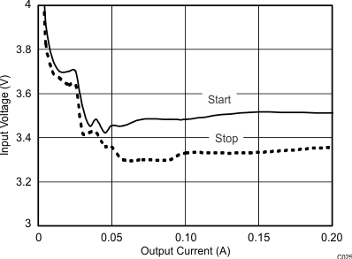
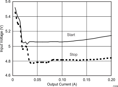
The start and stop voltages for typical 3.3-V and 5-V output applications are shown in Figure 25 and Figure 26. The voltages are plotted versus load current. The start voltage is defined as the input voltage needed to regulate the output within 1%. The stop voltage is defined as the input voltage at which the output drops by 5% or stops switching.
During high duty cycle conditions, the inductor current ripple increases while the BOOT capacitor is being recharged resulting in an increase in ripple voltage on the output. This is due to the recharge time of the boot capacitor being longer than the typical high-side off-time when switching occurs every cycle.
 Figure 25. 3.3V Start / Stop Voltage
  Figure 26. 5.0V Start / Stop Voltage