SLUS772G March 2008 – June 2020 TPS40210 , TPS40211
PRODUCTION DATA
- 1 Features
- 2 Applications
- 3 Description
- 4 Revision History
- 5 Pin Configuration and Functions
- 6 Specifications
-
7 Detailed Description
- 7.1 Overview
- 7.2 Functional Block Diagram
- 7.3
Feature Description
- 7.3.1 Soft Start
- 7.3.2 BP Regulator
- 7.3.3 Shutdown (DIS/ EN Pin)
- 7.3.4 Minimum On-Time and Off-Time Considerations
- 7.3.5 Setting the Oscillator Frequency
- 7.3.6 Synchronizing the Oscillator
- 7.3.7 Current Sense and Overcurrent
- 7.3.8 Current Sense and Subharmonic Instability
- 7.3.9 Current Sense Filtering
- 7.3.10 Control Loop Considerations
- 7.3.11 Gate Drive Circuit
- 7.3.12 TPS40211
- 7.4 Device Functional Modes
-
8 Application and Implementation
- 8.1 Application Information
- 8.2
Typical Applications
- 8.2.1
12-V to 24-V Nonsynchronous Boost Regulator
- 8.2.1.1 Design Requirements
- 8.2.1.2
Detailed Design Procedure
- 8.2.1.2.1 Custom Design with WEBENCH Tools
- 8.2.1.2.2 Duty Cycle Estimation
- 8.2.1.2.3 Inductor Selection
- 8.2.1.2.4 Rectifier Diode Selection
- 8.2.1.2.5 Output Capacitor Selection
- 8.2.1.2.6 Input Capacitor Selection
- 8.2.1.2.7 Current Sense and Current Limit
- 8.2.1.2.8 Current Sense Filter
- 8.2.1.2.9 Switching MOSFET Selection
- 8.2.1.2.10 Feedback Divider Resistors
- 8.2.1.2.11 Error Amplifier Compensation
- 8.2.1.2.12 RC Oscillator
- 8.2.1.2.13 Soft-Start Capacitor
- 8.2.1.2.14 Regulator Bypass
- 8.2.1.2.15 Bill of Materials
- 8.2.1.3 Application Curves
- 8.2.2 12-V Input, 700-mA LED Driver, Up to 35-V LED String
- 8.2.1
12-V to 24-V Nonsynchronous Boost Regulator
- 9 Power Supply Recommendations
- 10Layout
- 11Device and Documentation Support
- 12Mechanical, Packaging, and Orderable Information
封装选项
请参考 PDF 数据表获取器件具体的封装图。
机械数据 (封装 | 引脚)
- DRC|10
- DGQ|10
散热焊盘机械数据 (封装 | 引脚)
订购信息
7.3.8 Current Sense and Subharmonic Instability
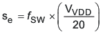
A characteristic of peak current mode control results in a condition where the current control loop can exhibit instability. This results in alternating long and short pulses from the pulse width modulator. The voltage loop maintains regulation and does not oscillate, but the output ripple voltage increases. The condition occurs only when the converter is operating in continuous conduction mode and the duty cycle is 50% or greater. The cause of this condition is described in the Modeling, Analysis and Compensation of the Current-Mode Converter Application Report. The remedy for this condition is to apply a compensating ramp from the oscillator to the signal going to the pulse width modulator. In the TPS40210 and TPS40211, the oscillator ramp is applied in a fixed amount to the pulse width modulator. The slope of the ramp is given in Equation 17.
To ensure that the converter does not enter into subharmonic instability, the slope of the compensating ramp signal must be at least half of the down slope of the current ramp signal. Since the compensating ramp is fixed in the TPS40210 and TPS40211, this places a constraint on the selection of the current sense resistor.
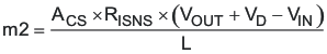
The down slope of the current sense wave form at the pulse width modulator is described in Equation 18.
Since the slope compensation ramp must be at least half, and preferably equal to the down slope of the current sense waveform seen at the pulse width modulator, a maximum value is placed on the current sense resistor when operating in continuous mode at 50% duty cycle or greater. For design purposes, some margin should be applied to the actual value of the current sense resistor. As a starting point, the actual resistor chosen should be 80% or less that the value calculated in Equation 19. This equation calculates the resistor value that makes the slope compensation ramp equal to one half of the current ramp downslope. Values no more than 80% of this result would be acceptable.
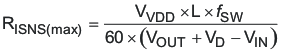
where
- Se is the slope of the voltage compensating ramp applied to the pulse width modulator in V/s
- fSW is the switching frequency in Hz
- VDD is the voltage at the VDD pin in V
- m2 is the down slope of the current sense waveform seen at the pulse width modulator in V/s
- RISNS is the value of the current sense resistor in Ω
- VOUT is the converter output voltage VIN is the converter power stage input voltage
- VD is the drop across the diode in Figure 7-7
It is possible to increase the voltage compensation ramp slope by connecting the VDD pin to the output voltage of the converter instead of the input voltage as shown in Figure 7-7. This can help in situations where the converter design calls for a large ripple current value in relation to the desired output current limit setting.
Connecting the VDD pin to the output voltage of the converter affects the start-up voltage of the converter since the controller undervoltage lockout (UVLO) circuit monitors the VDD pin and senses the input voltage less the diode drop before start-up. The effect is to increase the start-up voltage by the value of the diode voltage drop.
If an acceptable RISNS value is not available, the next higher value can be used and the signal from the resistor divided down to an acceptable level by placing another resistor in parallel with CIFLT.