SLUS772G March 2008 – June 2020 TPS40210 , TPS40211
PRODUCTION DATA
- 1 Features
- 2 Applications
- 3 Description
- 4 Revision History
- 5 Pin Configuration and Functions
- 6 Specifications
-
7 Detailed Description
- 7.1 Overview
- 7.2 Functional Block Diagram
- 7.3
Feature Description
- 7.3.1 Soft Start
- 7.3.2 BP Regulator
- 7.3.3 Shutdown (DIS/ EN Pin)
- 7.3.4 Minimum On-Time and Off-Time Considerations
- 7.3.5 Setting the Oscillator Frequency
- 7.3.6 Synchronizing the Oscillator
- 7.3.7 Current Sense and Overcurrent
- 7.3.8 Current Sense and Subharmonic Instability
- 7.3.9 Current Sense Filtering
- 7.3.10 Control Loop Considerations
- 7.3.11 Gate Drive Circuit
- 7.3.12 TPS40211
- 7.4 Device Functional Modes
-
8 Application and Implementation
- 8.1 Application Information
- 8.2
Typical Applications
- 8.2.1
12-V to 24-V Nonsynchronous Boost Regulator
- 8.2.1.1 Design Requirements
- 8.2.1.2
Detailed Design Procedure
- 8.2.1.2.1 Custom Design with WEBENCH Tools
- 8.2.1.2.2 Duty Cycle Estimation
- 8.2.1.2.3 Inductor Selection
- 8.2.1.2.4 Rectifier Diode Selection
- 8.2.1.2.5 Output Capacitor Selection
- 8.2.1.2.6 Input Capacitor Selection
- 8.2.1.2.7 Current Sense and Current Limit
- 8.2.1.2.8 Current Sense Filter
- 8.2.1.2.9 Switching MOSFET Selection
- 8.2.1.2.10 Feedback Divider Resistors
- 8.2.1.2.11 Error Amplifier Compensation
- 8.2.1.2.12 RC Oscillator
- 8.2.1.2.13 Soft-Start Capacitor
- 8.2.1.2.14 Regulator Bypass
- 8.2.1.2.15 Bill of Materials
- 8.2.1.3 Application Curves
- 8.2.2 12-V Input, 700-mA LED Driver, Up to 35-V LED String
- 8.2.1
12-V to 24-V Nonsynchronous Boost Regulator
- 9 Power Supply Recommendations
- 10Layout
- 11Device and Documentation Support
- 12Mechanical, Packaging, and Orderable Information
封装选项
请参考 PDF 数据表获取器件具体的封装图。
机械数据 (封装 | 引脚)
- DRC|10
- DGQ|10
散热焊盘机械数据 (封装 | 引脚)
订购信息
8.2.1.2.11 Error Amplifier Compensation
Compensation selection can be done with aid of WEBENCH to select compensation components or with the aid of the average Spice model to simulate the open loop modulator and power stage gain. Alternatively, the following procedure gives a good starting point.
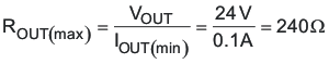
While current mode control typically only requires Type II compensation, it is desirable to layout for Type III compensation to increase flexibility during design and development. Current mode control boost converters have higher gain with higher output impedance, so it is necessary to calculate the control loop gain at the maximum output impedance, estimated by Equation 58.
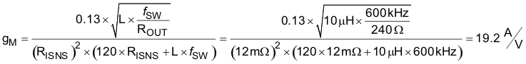
The transconductance of the TPS40210 current mode control can be estimated by Equation 59.
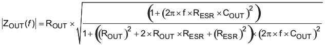
The maximum output impedance ZOUT, can be estimated by Equation 60.
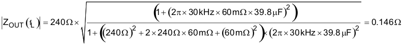
At the desired crossover frequency (fL) of 30 kHz, ZOUT becomes 0.146 Ω.
The modulator gain at the desired cross-over can be estimated by Equation 62.

The feedback compensation network needs to be designed to provide an inverse gain at the cross-over frequency for unity loop gain. This sets the compensation mid-band gain at a value calculated in Equation 63.
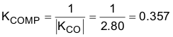
To set the mid-band gain of the error amplifier to KCOMP, use Equation 64.
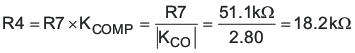
R4 = 18.7 kΩ selected.
Place the zero at 1/10th of the desired cross-over frequency.
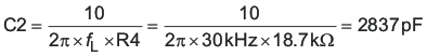
C2 = 2200 pF selected.
Place a high-frequency pole at about five times the desired cross-over frequency and less than one-half the unity gain bandwidth of the error amplifier:
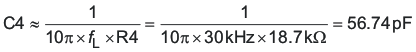
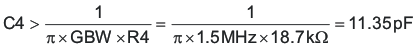
C4 = 47 pF selected.