ZHCSJX1B NOVEMBER 2008 – June 2019 TPS40197
PRODUCTION DATA.
8.3.1 Enable
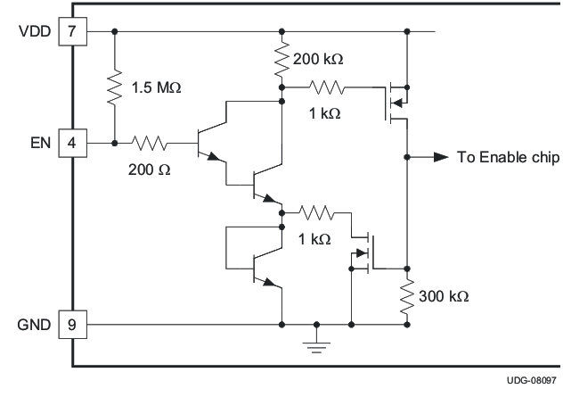
The TPS40197 includes a dedicated EN pin. This simplifies user level interface design since no multiplexed functions exist. Another benefit is a true low-power shutdown mode of operation. When the EN pin is pulled to GND, all unnecessary functions, including the BP regulator, are turned off, reducing the IVDD current to 45 μA. A functionally equivalent circuit of the enable circuitry is shown in Figure 14.
 Figure 14. Tps40197 En Pin Internal Circuitry
 If the EN pin is left floating, the device starts automatically. The pin must be pulled to less than 600 mV to specify that the TPS40197 is in shutdown mode. Note that the EN pin is relatively high impedance. In some situations, there could be enough noise nearby to cause the EN pin to swing below the 600-mV threshold and give erroneous shutdown commands to other components of the device. There are two solutions to this potential problem.
- Place a capacitor from EN to GND. A side-effect of this is to delay the start of the converter while the capacitor charges past the enable threshold.
- Place a resistor from VDD to EN. This causes more current to flow in the shutdown mode, but does not delay converter start-up. If a resistor is used, the total current into the EN pin must be limited to no more than 500 μA.
The ENABLE pin is self clamping. The clamp voltage can be as low as 1 V with a 1-kΩ ground impedance. Due to this self-clamping feature, the pull-up impedance on the ENABLE pin should be selected to limit the sink current to less than 500 μA. Driving the ENABLE pin with a low-impedance source voltage can result in damage to the device. Because of the self-clamping feature, it requires care when connecting multiple ENABLE pins together. For enabling multiple TPS4019x devices (TPS40190, TPS40192, TPS40193, TPS40195, TPS40197), see application report SLVA509.