ZHCSAK8J December 2003 – June 2022 TPS40054 , TPS40055 , TPS40057
PRODUCTION DATA
- 1 特性
- 2 应用
- 3 说明
- 4 Revision History
- 5 Pin Configuration and Functions
- 6 Specifications
-
7 Detailed Description
- 7.1 Overview
- 7.2 Functional Block Diagram
- 7.3
Feature Description
- 7.3.1 Setting the Switching Frequency (Programming the Clock Oscillator)
- 7.3.2 Programming The Ramp Generator Circuit
- 7.3.3 UVLO Operation
- 7.3.4 BP5 and BP10 Internal Voltage Regulators
- 7.3.5 Programming Soft Start
- 7.3.6 Programming Current Limit
- 7.3.7 Synchronizing to an External Supply
- 7.3.8 Loop Compensation
- 7.4 Device Functional Modes
-
8 Application and Implementation
- 8.1 Application Information
- 8.2
Typical Application
- 8.2.1 Design Requirements
- 8.2.2
Detailed Design Procedure
- 8.2.2.1 Calculate Maximum and Minimum Duty Cycles
- 8.2.2.2 Select Switching Frequency
- 8.2.2.3 Select ΔI
- 8.2.2.4 Calculate the High-Side MOSFET Power Losses
- 8.2.2.5 Calculate Synchronous Rectifier Losses
- 8.2.2.6 Calculate the Inductor Value
- 8.2.2.7 Set the Switching Frequency
- 8.2.2.8 Program the Ramp Generator Circuit
- 8.2.2.9 Calculate the Output Capacitance (CO)
- 8.2.2.10 Calculate the Soft-Start Capacitor (CSS/SD)
- 8.2.2.11 Calculate the Current Limit Resistor (RILIM)
- 8.2.2.12 Calculate Loop Compensation Values
- 8.2.2.13 Calculate the Boost and BP10V Bypass Capacitance
- 8.2.3 Application Curves
- 9 Power Supply Recommendations
- 10Layout
- 11Device and Documentation Support
- 12Mechanical, Packaging, and Orderable Information
封装选项
请参考 PDF 数据表获取器件具体的封装图。
机械数据 (封装 | 引脚)
- PWP|16
散热焊盘机械数据 (封装 | 引脚)
- PWP|16
订购信息
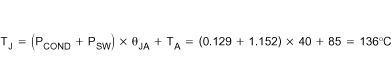
8.2.2.4 Calculate the High-Side MOSFET Power Losses
Power losses in the high-side MOSFET (Si7860DP) at 24-VIN where switching losses dominate can be calculated from Equation 52.
Equation 52. 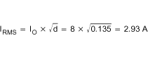
Substituting Equation 34 into Equation 33 yields
Equation 53. 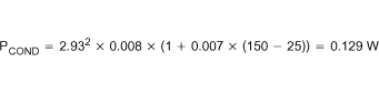
and from Equation 35, the switching losses can be determined.
Equation 54. 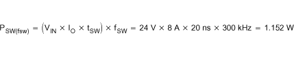
The MOSFET junction temperature can be found by substituting Equation 53 and Equation 54 into Equation 36:
Equation 55.