ZHCSAK8J December 2003 – June 2022 TPS40054 , TPS40055 , TPS40057
PRODUCTION DATA
- 1 特性
- 2 应用
- 3 说明
- 4 Revision History
- 5 Pin Configuration and Functions
- 6 Specifications
-
7 Detailed Description
- 7.1 Overview
- 7.2 Functional Block Diagram
- 7.3
Feature Description
- 7.3.1 Setting the Switching Frequency (Programming the Clock Oscillator)
- 7.3.2 Programming The Ramp Generator Circuit
- 7.3.3 UVLO Operation
- 7.3.4 BP5 and BP10 Internal Voltage Regulators
- 7.3.5 Programming Soft Start
- 7.3.6 Programming Current Limit
- 7.3.7 Synchronizing to an External Supply
- 7.3.8 Loop Compensation
- 7.4 Device Functional Modes
-
8 Application and Implementation
- 8.1 Application Information
- 8.2
Typical Application
- 8.2.1 Design Requirements
- 8.2.2
Detailed Design Procedure
- 8.2.2.1 Calculate Maximum and Minimum Duty Cycles
- 8.2.2.2 Select Switching Frequency
- 8.2.2.3 Select ΔI
- 8.2.2.4 Calculate the High-Side MOSFET Power Losses
- 8.2.2.5 Calculate Synchronous Rectifier Losses
- 8.2.2.6 Calculate the Inductor Value
- 8.2.2.7 Set the Switching Frequency
- 8.2.2.8 Program the Ramp Generator Circuit
- 8.2.2.9 Calculate the Output Capacitance (CO)
- 8.2.2.10 Calculate the Soft-Start Capacitor (CSS/SD)
- 8.2.2.11 Calculate the Current Limit Resistor (RILIM)
- 8.2.2.12 Calculate Loop Compensation Values
- 8.2.2.13 Calculate the Boost and BP10V Bypass Capacitance
- 8.2.3 Application Curves
- 9 Power Supply Recommendations
- 10Layout
- 11Device and Documentation Support
- 12Mechanical, Packaging, and Orderable Information
封装选项
请参考 PDF 数据表获取器件具体的封装图。
机械数据 (封装 | 引脚)
- PWP|16
散热焊盘机械数据 (封装 | 引脚)
- PWP|16
订购信息
7.3.6 Programming Current Limit
The TPS4005x uses a two-tier approach for overcurrent protection. The first tier is a pulse-by-pulse protection scheme. Current limit is implemented on the high-side MOSFET by sensing the voltage drop across the MOSFET when the gate is driven high. The MOSFET voltage is compared to the voltage dropped across a resistor connected from VIN pin to the ILIM pin when driven by a constant current sink. If the voltage drop across the MOSFET exceeds the voltage drop across the ILIM resistor, the switching pulse is immediately terminated. The MOSFET remains off until the next switching cycle is initiated.
The second tier consists of a fault counter. The fault counter is incremented on an overcurrent pulse and decremented on a clock cycle without an overcurrent pulse. When the counter reaches seven, a restart is issued and seven soft-start cycles are initiated. Both the upper and lower MOSFETs are turned off during this period. The counter is decremented on each soft-start cycle. When the counter is decremented to zero, the PWM is re-enabled. If the fault has been removed, the output starts up normally. If the output is still present, the counter counts seven overcurrent pulses and re-enters the second-tier fault mode. See Figure 7-4 for typical overcurrent protection waveforms.
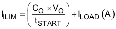
The minimum current limit setpoint (IILIM) is calculated in Equation 7.
where
- ILOAD is the load current at start-up.
 Figure 7-4 Typical Current Limit Protection Waveforms
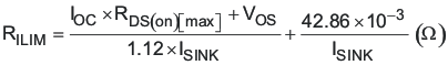
The current limit programming resistor (RILIM) is calculated using Equation 8. Care must be taken in choosing the values used for VOS and ISINK in the equation. To ensure the output current at the overcurrent level, the minimum value of ISINK and the maximum value of VOS must be used. The main purpose is hard fault protection of the power switches.
where
- ISINK is the current into the ILIM pin and is 8.5 μA, minimum.
- IOC is the overcurrent setpoint, which is the DC output current plus one-half of the peak inductor current.
- VOS is the overcurrent comparator offset and is –20 mV maximum.