ZHCSAK8J December 2003 – June 2022 TPS40054 , TPS40055 , TPS40057
PRODUCTION DATA
- 1 特性
- 2 应用
- 3 说明
- 4 Revision History
- 5 Pin Configuration and Functions
- 6 Specifications
-
7 Detailed Description
- 7.1 Overview
- 7.2 Functional Block Diagram
- 7.3
Feature Description
- 7.3.1 Setting the Switching Frequency (Programming the Clock Oscillator)
- 7.3.2 Programming The Ramp Generator Circuit
- 7.3.3 UVLO Operation
- 7.3.4 BP5 and BP10 Internal Voltage Regulators
- 7.3.5 Programming Soft Start
- 7.3.6 Programming Current Limit
- 7.3.7 Synchronizing to an External Supply
- 7.3.8 Loop Compensation
- 7.4 Device Functional Modes
-
8 Application and Implementation
- 8.1 Application Information
- 8.2
Typical Application
- 8.2.1 Design Requirements
- 8.2.2
Detailed Design Procedure
- 8.2.2.1 Calculate Maximum and Minimum Duty Cycles
- 8.2.2.2 Select Switching Frequency
- 8.2.2.3 Select ΔI
- 8.2.2.4 Calculate the High-Side MOSFET Power Losses
- 8.2.2.5 Calculate Synchronous Rectifier Losses
- 8.2.2.6 Calculate the Inductor Value
- 8.2.2.7 Set the Switching Frequency
- 8.2.2.8 Program the Ramp Generator Circuit
- 8.2.2.9 Calculate the Output Capacitance (CO)
- 8.2.2.10 Calculate the Soft-Start Capacitor (CSS/SD)
- 8.2.2.11 Calculate the Current Limit Resistor (RILIM)
- 8.2.2.12 Calculate Loop Compensation Values
- 8.2.2.13 Calculate the Boost and BP10V Bypass Capacitance
- 8.2.3 Application Curves
- 9 Power Supply Recommendations
- 10Layout
- 11Device and Documentation Support
- 12Mechanical, Packaging, and Orderable Information
封装选项
请参考 PDF 数据表获取器件具体的封装图。
机械数据 (封装 | 引脚)
- PWP|16
散热焊盘机械数据 (封装 | 引脚)
- PWP|16
订购信息
7.3.5 Programming Soft Start
The TPS4005x uses a closed-loop soft-start system to ensure a controlled ramp of the output during start-up. The reference voltage used for the start-up is derived in the following manner. A capacitor (CSS/SD) is connected to the SS/SD pin. There is a ramped voltage generated at this pin by charging CSS/SD with a current source. A value of 0.85 V is subtracted from the voltage at the SS/SSD pin and is applied to a non-inverting input of the error amplifier. This is the effective soft-start ramp voltage, VSSRMP. The error amplifier also has the 0.7-V reference (VFB) voltage applied to a non-inverting input. The structure of the error amplifier input stage is such that the lower of VFB or VSSRMP becomes the dominant voltage that the error amplifier uses to regulate the FB pin. This provides a clean, closed-loop start-up while VSSRMP is lower than VFB and a precision reference regulated supply as VSSRMP climbs above VFB. To ensure a controlled ramp-up of the output voltage, the soft-start time must be greater than the L-CO time constant as described in Equation 5.
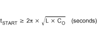
where
- tSTART is the start-up ramp time in s.
There is a direct correlation between tSTART and the input current required during start-up. The faster tSTART, the higher the input current required during start-up. This relationship is described in more detail in the Programming the Current Limit section. The soft-start capacitance, CSS/SD, is described in Equation 6.
For applications in which the VIN supply ramps up slowly (typically between 50 ms and 100 ms), it can be necessary to increase the soft-start time to between approximately 2 ms and 5 ms to prevent nuisance UVLO tripping. The soft-start time must be longer than the time that the VIN supply transitions between 6 V and 7 V.
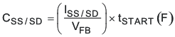
where
- ISS/SD is the soft-start charge current (typical value is 2.35 μA).
- VFB is the feedback reference voltage (typical value is 0.7 V).