ZHCSAK8J December 2003 – June 2022 TPS40054 , TPS40055 , TPS40057
PRODUCTION DATA
- 1 特性
- 2 应用
- 3 说明
- 4 Revision History
- 5 Pin Configuration and Functions
- 6 Specifications
-
7 Detailed Description
- 7.1 Overview
- 7.2 Functional Block Diagram
- 7.3
Feature Description
- 7.3.1 Setting the Switching Frequency (Programming the Clock Oscillator)
- 7.3.2 Programming The Ramp Generator Circuit
- 7.3.3 UVLO Operation
- 7.3.4 BP5 and BP10 Internal Voltage Regulators
- 7.3.5 Programming Soft Start
- 7.3.6 Programming Current Limit
- 7.3.7 Synchronizing to an External Supply
- 7.3.8 Loop Compensation
- 7.4 Device Functional Modes
-
8 Application and Implementation
- 8.1 Application Information
- 8.2
Typical Application
- 8.2.1 Design Requirements
- 8.2.2
Detailed Design Procedure
- 8.2.2.1 Calculate Maximum and Minimum Duty Cycles
- 8.2.2.2 Select Switching Frequency
- 8.2.2.3 Select ΔI
- 8.2.2.4 Calculate the High-Side MOSFET Power Losses
- 8.2.2.5 Calculate Synchronous Rectifier Losses
- 8.2.2.6 Calculate the Inductor Value
- 8.2.2.7 Set the Switching Frequency
- 8.2.2.8 Program the Ramp Generator Circuit
- 8.2.2.9 Calculate the Output Capacitance (CO)
- 8.2.2.10 Calculate the Soft-Start Capacitor (CSS/SD)
- 8.2.2.11 Calculate the Current Limit Resistor (RILIM)
- 8.2.2.12 Calculate Loop Compensation Values
- 8.2.2.13 Calculate the Boost and BP10V Bypass Capacitance
- 8.2.3 Application Curves
- 9 Power Supply Recommendations
- 10Layout
- 11Device and Documentation Support
- 12Mechanical, Packaging, and Orderable Information
封装选项
请参考 PDF 数据表获取器件具体的封装图。
机械数据 (封装 | 引脚)
- PWP|16
散热焊盘机械数据 (封装 | 引脚)
- PWP|16
订购信息
7.3.2 Programming The Ramp Generator Circuit
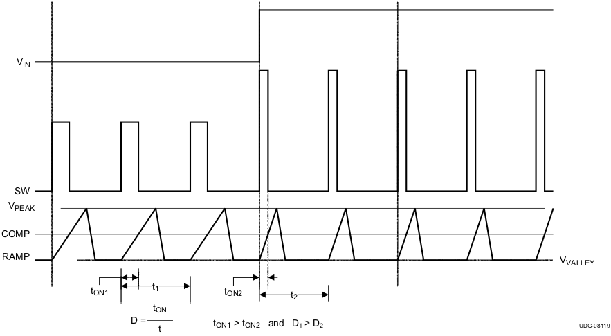
The ramp generator circuit provides the actual ramp used by the PWM comparator. The ramp generator provides voltage feedforward control by varying the PWM ramp slope with line voltage, while maintaining a constant ramp magnitude. Varying the PWM ramp directly with line voltage provides excellent response to line variations because the PWM does not have to wait for loop delays before changing the duty cycle (see Figure 7-1).
 Figure 7-1 Voltage Feedforward
Effect on PWM Duty Cycle
Figure 7-1 Voltage Feedforward
Effect on PWM Duty CycleThe PWM ramp must be faster than the controller clock frequency or the PWM is prevented from starting. The PWM ramp time is programmed through a single resistor (RKFF) pulled up to VIN. RKFF is related to RT, and the minimum input voltage, VIN(min), through the following:

where
- VIN(min) is the ensured minimum start-up voltage (the actual start-up voltage is nominally about 10% lower at 25°C). VIN(min) must be programmed equal to or greater than 8 V to ensure start-up and shutdown through the programmed UVLO through the KFF pin.
- RT is the timing resistance in kΩ.
- VKFF is the voltage at the KFF pin (typical value is 3.48 V).
The curve showing the RKFF required for a given switching frequency, fSW, and VUVLO is shown in Figure 6-2.
For low-input voltage and high duty-cycle applications, the voltage feedforward can limit the duty cycle prematurely, but does not occur for most applications. The voltage control loop controls the duty cycle and regulates the output voltage. For more information on large duty cycle operation, refer to the Effect of Programmable UVLO on Maximum Duty Cycle application note.