ZHCSAK8J December 2003 – June 2022 TPS40054 , TPS40055 , TPS40057
PRODUCTION DATA
- 1 特性
- 2 应用
- 3 说明
- 4 Revision History
- 5 Pin Configuration and Functions
- 6 Specifications
-
7 Detailed Description
- 7.1 Overview
- 7.2 Functional Block Diagram
- 7.3
Feature Description
- 7.3.1 Setting the Switching Frequency (Programming the Clock Oscillator)
- 7.3.2 Programming The Ramp Generator Circuit
- 7.3.3 UVLO Operation
- 7.3.4 BP5 and BP10 Internal Voltage Regulators
- 7.3.5 Programming Soft Start
- 7.3.6 Programming Current Limit
- 7.3.7 Synchronizing to an External Supply
- 7.3.8 Loop Compensation
- 7.4 Device Functional Modes
-
8 Application and Implementation
- 8.1 Application Information
- 8.2
Typical Application
- 8.2.1 Design Requirements
- 8.2.2
Detailed Design Procedure
- 8.2.2.1 Calculate Maximum and Minimum Duty Cycles
- 8.2.2.2 Select Switching Frequency
- 8.2.2.3 Select ΔI
- 8.2.2.4 Calculate the High-Side MOSFET Power Losses
- 8.2.2.5 Calculate Synchronous Rectifier Losses
- 8.2.2.6 Calculate the Inductor Value
- 8.2.2.7 Set the Switching Frequency
- 8.2.2.8 Program the Ramp Generator Circuit
- 8.2.2.9 Calculate the Output Capacitance (CO)
- 8.2.2.10 Calculate the Soft-Start Capacitor (CSS/SD)
- 8.2.2.11 Calculate the Current Limit Resistor (RILIM)
- 8.2.2.12 Calculate Loop Compensation Values
- 8.2.2.13 Calculate the Boost and BP10V Bypass Capacitance
- 8.2.3 Application Curves
- 9 Power Supply Recommendations
- 10Layout
- 11Device and Documentation Support
- 12Mechanical, Packaging, and Orderable Information
封装选项
请参考 PDF 数据表获取器件具体的封装图。
机械数据 (封装 | 引脚)
- PWP|16
散热焊盘机械数据 (封装 | 引脚)
- PWP|16
订购信息
7.3.7 Synchronizing to an External Supply
The TPS4005x can be synchronized to an external clock through the SYNC pin. Synchronization occurs on the falling edge of the SYNC signal. The synchronization frequency must be in the range of 20% to 30% higher than its programmed free-run frequency. The clock frequency at the SYNC pin replaces the controller clock generated by the oscillator circuit. Pulling the SYNC pin low programs the TPS4005x to freely run at the frequency programmed by RT.
The higher synchronization must be factored in when programming the PWM ramp generator circuit. If the PWM ramp is interrupted by the SYNC pulse, a UVLO condition is declared and the PWM becomes disabled. Typically, this is of concern under low-line conditions only. In any case, RKFF needs to be adjusted for the higher switching frequency. In order to specify the correct value for RKFF at the synchronizing frequency, calculate a dummy value for RT that would cause the oscillator to run at the synchronizing frequency. Do not use this value of RT in the design.
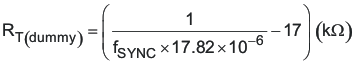
where
- fSYNC is the synchronizing frequency in kHz.
Use the value of RT(dummy) to calculate the value for RKFF.

where
- RT(dummy) is in kΩ.
This value of RKFF ensures that UVLO is not engaged when operating at the synchronization frequency.