ZHCSNR4B May 2021 – April 2022 TPS25946
PRODUCTION DATA
- 1 特性
- 2 应用
- 3 说明
- 4 Revision History
- 5 Device Comparison Table
- 6 Pin Configuration and Functions
- 7 Specifications
-
8 Detailed Description
- 8.1 Overview
- 8.2 Functional Block Diagram
- 8.3
Feature Description
- 8.3.1 Undervoltage Lockout (UVLO and UVP)
- 8.3.2 Overvoltage Lockout (OVLO)
- 8.3.3 Inrush Current, Overcurrent, and Short-Circuit Protection
- 8.3.4 Analog Load Current Monitor
- 8.3.5 Reverse Current Protection
- 8.3.6 Overtemperature Protection (OTP)
- 8.3.7 Fault Response and Indication (FLT)
- 8.3.8 Power Good Indication (PG)
- 8.3.9 Input Supply Good Indication (SPLYGD)
- 8.4 Device Functional Modes
-
9 Application and Implementation
- 9.1 Application Information
- 9.2
Typical Application
- 9.2.1 Design Requirements
- 9.2.2
Detailed Design Procedure
- 9.2.2.1 Device Selection
- 9.2.2.2 Setting Overvoltage Threshold
- 9.2.2.3 Setting Output Voltage Rise Time (tR)
- 9.2.2.4 Setting Power Good Assertion Threshold
- 9.2.2.5 Setting Overcurrent Threshold (ILIM)
- 9.2.2.6 Setting Overcurrent Blanking Interval (tITIMER)
- 9.2.2.7 Selecting External Bias Resistor (R5)
- 9.2.2.8 Selecting External Diode (D1)
- 9.2.3 Application Curve
- 10Power Supply Recommendations
- 11Layout
- 12Device and Documentation Support
- 13Mechanical, Packaging, and Orderable Information
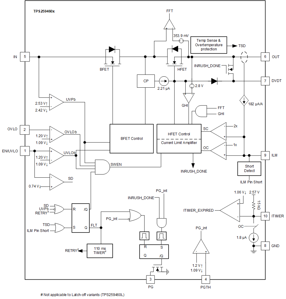
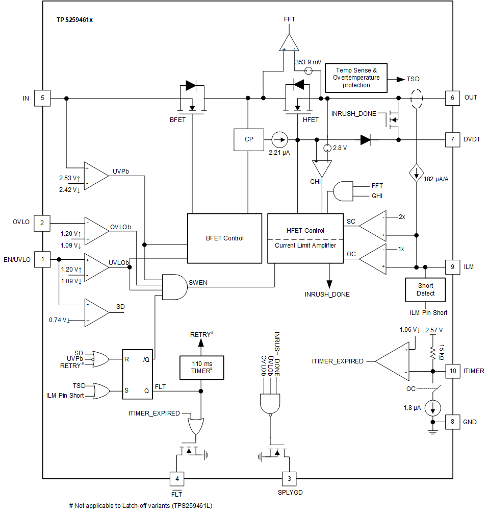
8.2 Functional Block Diagram
 Figure 8-1 TPS259460x Block
Diagram
 Figure 8-2 TPS259461x Block Diagram