ZHCSP87A December 2022 – September 2023 TPS25772-Q1
PRODUCTION DATA
- 1
- 1 特性
- 2 应用
- 3 说明
- 4 Revision History
- 5 Device Comparison Table
- 6 Pin Configuration and Functions
-
7 Specifications
- 7.1 Absolute Maximum Ratings
- 7.2 ESD Ratings
- 7.3 Recommended Operating Conditions
- 7.4 Recommended Components
- 7.5 Thermal Information
- 7.6 Buck-Boost Regulator
- 7.7 CC Cable Detection Parameters
- 7.8 CC VCONN Parameters
- 7.9 CC PHY Parameters
- 7.10 Thermal Shutdown Characteristics
- 7.11 Oscillator Characteristics
- 7.12 ADC Characteristics
- 7.13 TVS Parameters
- 7.14 Input/Output (I/O) Characteristics
- 7.15 BC1.2 Characteristics
- 7.16 I2C Requirements and Characteristics
- 7.17 Typical Characteristics
- 8 Parameter Measurement Information
-
9 Detailed Description
- 9.1 Overview
- 9.2 Functional Block Diagram
- 9.3
Feature Description
- 9.3.1 Device Power Management and Supervisory Circuitry
- 9.3.2 TVSP Device Configuration and ESD Protection
- 9.3.3
Buck-Boost Regulator
- 9.3.3.1 Buck-Boost Regulator Operation
- 9.3.3.2 Switching Frequency, Frequency Dither, Phase-Shift and Synchronization
- 9.3.3.3 VIN Supply and VIN Over-Voltage Protection
- 9.3.3.4 Feedback Paths and Error Amplifiers
- 9.3.3.5 Transconductors and Compensation
- 9.3.3.6 Output Voltage DAC, Soft-Start and Cable Droop Compensation
- 9.3.3.7 VBUS Overvoltage Protection
- 9.3.3.8 VBUS Undervoltage Protection
- 9.3.3.9 Current Sense Resistor (RSNS) and Current Limit Operation
- 9.3.3.10 Buck-Boost Peak Current Limits
- 9.3.4 USB-PD Physical Layer
- 9.3.5 VCONN
- 9.3.6 Cable Plug and Orientation Detection
- 9.3.7 ADC
- 9.3.8 BC 1.2, Legacy and Fast Charging Modes (Px_DP, Px_DM)
- 9.3.9 USB2.0 Low-Speed Endpoint
- 9.3.10 Digital Interfaces
- 9.3.11 I2C Interface
- 9.3.12 Digital Core
- 9.3.13 NTC Input
- 9.3.14 Thermal Sensors and Thermal Shutdown
- 9.4 Device Functional Modes
- 10Application and Implementation
- 11Device and Documentation Support
- 12Mechanical, Packaging, and Orderable Information
9.3.1.1 VIN UVLO and Enable/UVLO
The TPS25772-Q1 has one internally fixed VIN UVLO and one user programmable UVLO using the EN/UVLO pin. Both thresholds must be cleared for the device to start up.
- The fixed VIN(UVLO) has a rising threshold between 5 and 5.5 V to ensure internal circuits have sufficient headroom for proper operation.
- The EN/UVLO pin provides the user with a resistor programmable UVLO threshold and master enable / disable for the device.
The EN/UVLO pin has three distinct voltage ranges: shutdown, standby, and operating. When the EN/UVLO pin is below the standby threshold VEN(STBY), the device is disabled in a low power shutdown. When EN/UVLO voltage is greater than the standby threshold VEN(STBY) but less than the operating threshold VEN(OPER), the internal bias rails, LDO_5V, LDO_3V3, and LDO_1V5 regulators are enabled but remaining device functions are disabled. When EN/UVLO is greater than the operating threshold VEN(OPER) and LDO_5V, LDO_3V3 and LDO_1V5 regulators are above their respective undervoltage threshold UVLO thresholds, the device is fully functional. The EN/UVLO pin includes fixed hysteresis between the shutdown mode and the standby mode.
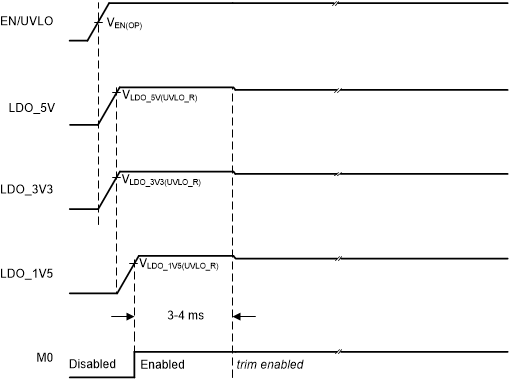
| EN/UVLO (1) | LDOs | DEVICE OPERATION |
|---|---|---|
| VEN/UVLO < VEN(LDO_V5V_F) | — | Shutdown: LDO_5V, LDO_3V3 and LDO_1V5 OFF. M0 (MCU) is OFF. |
| VEN(LDO_V5V_R) < VEN/UVLO < VEN(STBY) | — | Standby: LDO_5V, LDO_3V3 and LDO_1V5 ON. M0 (MCU) is OFF. |
| VEN/UVLO > VEN(OPER) | LDO_5V < VLDO_5V(UVLO_R), or LDO_3V3 < VLDO_3V3(UVLO_R); or LDO_1V5 < VLDO_1V5(UVLO_R) | LDO_5V, LDO_3V3 and LDO_1V5 ON, M0 (MCU) is OFF. |
| VEN/UVLO > VEN(OPER) | LDO_5V > VLDO_5V(UVLO_R), and LDO_3V3 > VLDO_3V3(UVLO_R), and LDO_1V5 > VLDO_1V5(UVLO_R) | Operating: M0 (MCU) is ON. |
In some cases an input UVLO level different than that provided by the internal VIN(UVLO) is needed. This can be accomplished by using the circuit shown in UVLO Threshold Programming. The input voltage at which the device turns on is designated VON; while the turnoff voltage is VOFF. First a value for RENB is chosen in the range of 13 kΩ to 22 kΩ. Use Equation 3 and Equation 7 to calculate RENT and VOFF.
The hysteresis between the UVLO turn-on threshold and turn-off threshold is set by the upper resistor in the EN/UVLO resistor divider and is given by:
 Figure 9-2 UVLO Threshold Programming
Where
- VON = VIN turn-on voltage
- VOFF = VIN turn-off voltage
If the programmable UVLO is not required, the EN/UVLO pin can be connected to the IN pin with a 47 kΩ, or larger, resistor.