ZHCSMU0D July 2009 – December 2020 TPS23753A
PRODUCTION DATA
- 1 特性
- 2 应用
- 3 说明
- 4 Revision History
- 5 Product Information
- 6 Pin Configuration and Functions
- 7 Specifications
-
8 Detailed Description
- 8.1 Overview
- 8.2 Functional Block Diagram
- 8.3 Feature Description
- 8.4
Device Functional Modes
- 8.4.1 Threshold Voltages
- 8.4.2 PoE Start-Up Sequence
- 8.4.3 Detection
- 8.4.4 Hardware Classification
- 8.4.5 Maintain Power Signature (MPS)
- 8.4.6 TPS23753A Operation
- 8.4.7 Special Switching MOSFET Considerations
- 8.4.8 Thermal Considerations
- 8.4.9 FRS and Synchronization
- 8.4.10 Blanking – RBLNK
- 8.4.11 Current Slope Compensation
- 8.4.12 Adapter ORing
- 8.4.13 Protection
- 8.4.14 Frequency Dithering for Conducted Emissions Control
- 9 Application and Implementation
- 10Power Supply Recommendations
- 11Layout
- 12Device and Documentation Support
- 13Mechanical, Packaging, and Orderable Information
8.4.6.1 Start-Up and Converter Operation
The internal PoE undervoltage lockout (UVLO) circuit holds the hotswap switch off before the PSE provides full voltage to the PD. This prevents the converter circuits from loading the PoE input during detection and classification. The converter circuits discharges CIN, CVC, and CVB while the PD is unpowered. Thus VRTN-VDD will be a small voltage just after full voltage is applied to the PD, as seen in Figure 8-3.
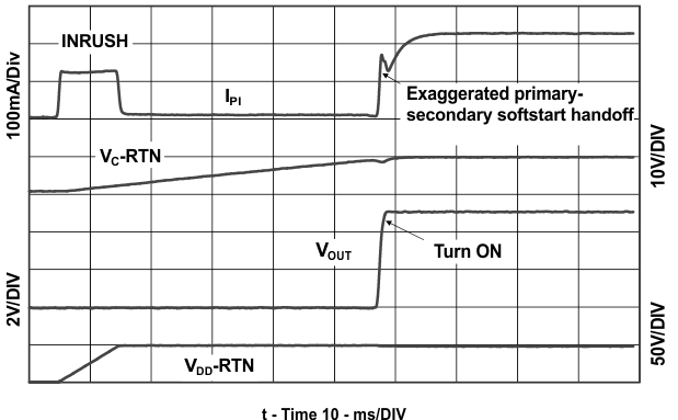
The PSE drives the PI voltage to the operating range once it has decided to power up the PD. When VDD rises above the UVLO turnon threshold (VUVLO-R, approximately 35 V) with RTN high, the TPS23753A enables the hotswap MOSFET with an approximately 140-mA (inrush) current limit. See the waveforms of Figure 8-4 for an example. Converter switching is disabled while CIN charges and VRTN falls from VDD to nearly VSS; however, the converter start-up circuit is allowed to charge CVC. Once the inrush current falls about 10% below the inrush current limit, the PD control switches to the operational level (approximately 450 mA) and converter switching is permitted.
Converter switching is allowed if the PD is not in inrush and the VC UVLO circuit permits it. Continuing the start-up sequence shown in Figure 8-4, VVC rises as the start-up current source charges CVC and M1 switching is inhibited by the status of the VC UVLO. The VB regulator powers the internal converter circuits as VVC rises. Start-up current is turned off, converter switching is enabled, and a soft-start cycle starts when VVC exceeds UVLO1 (approximately 9 V). VVC falls as it powers both the internal circuits and the switching MOSFET gate. If the converter control-bias output rises to support VVC before it falls to UVLO1 – UVLO1H (approximately 5.5 V), a successful start-up occurs. Figure 8-4 shows a small droop in VVC while the output voltage rises smoothly and a successful start-up occurs.
 Figure 8-4 Power Up and Start
If VVDD-VSS drops below the lower PoE UVLO (UVLOR – UVLOH, approximately 30.5 V), the hotswap MOSFET is turned off, but the converter still runs. The converter stops if VVC falls below the converter UVLO (UVLO1 – UVLOH, approximately 5.5 V), the hotswap is in inrush current limit, or 0% duty cycle is demanded by VCTL (VCTL < VZDC, approximately 1.5 V), or the converter is in thermal shutdown.