ZHCSCB9E April   2014  – July 2022 TPS22965-Q1

PRODUCTION DATA  

  1. 特性
  2. 应用
  3. 说明
  4. Revision History
  5. Device Comparison Table
  6. Pin Configuration and Functions
  7. Specifications
    1. 7.1 Absolute Maximum Ratings
    2. 7.2 ESD Ratings
    3. 7.3 Recommended Operating Conditions
    4. 7.4 Thermal Information
    5. 7.5 Electrical Characteristics—VBIAS = 5 V
    6. 7.6 Electrical Characteristics—VBIAS = 2.5 V
    7. 7.7 Switching Characteristics
    8. 7.8 Typical Characteristics
      1. 7.8.1 Typical DC Characteristics
      2. 7.8.2 Typical Switching Characteristics
  8. Parameter Measurement Information
  9. Detailed Description
    1. 9.1 Overview
    2. 9.2 Functional Block Diagram
    3. 9.3 Feature Description
      1. 9.3.1 Adjustable Rise Time
      2. 9.3.2 Quick Output Discharge (TPS22965-Q1 and TPS22965W-Q1 Only)
      3. 9.3.3 Low Power Consumption During OFF State
    4. 9.4 Device Functional Modes
  10. 10Application and Implementation
    1. 10.1 Application Information
      1. 10.1.1 VIN to VOUT Voltage Drop
      2. 10.1.2 On and Off Control
      3. 10.1.3 Input Capacitor (Optional)
      4. 10.1.4 Output Capacitor (Optional)
      5. 10.1.5 VIN and VBIAS Voltage Range
    2. 10.2 Typical Application
      1. 10.2.1 Design Requirements
      2. 10.2.2 Detailed Design Procedure
        1. 10.2.2.1 Inrush Current
      3. 10.2.3 Application Curves
  11. 11Power Supply Recommendations
  12. 12Layout
    1. 12.1 Layout Guidelines
    2. 12.2 Layout Example
    3. 12.3 Thermal Consideration
  13. 13Device and Documentation Support
    1. 13.1 Documentation Support
      1. 13.1.1 Related Documentation
    2. 13.2 接收文档更新通知
    3. 13.3 支持资源
    4. 13.4 Trademarks
    5. 13.5 Electrostatic Discharge Caution
    6. 13.6 术语表
  14. 14Mechanical, Packaging, and Orderable Information

封装选项

机械数据 (封装 | 引脚)
散热焊盘机械数据 (封装 | 引脚)
订购信息

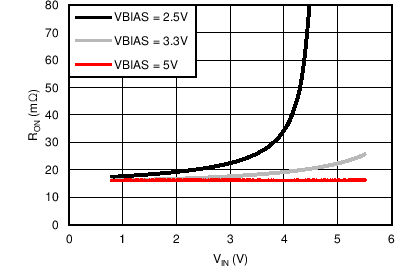
VIN and VBIAS Voltage Range

For optimal RON performance, make sure VIN ≤ VBIAS. The device is still functional if VIN > VBIAS but it exhibits RON greater than what is listed in the Electrical Characteristics—VBIAS = 2 V to 2.5 V table. See the following figure for an example of a typical device. Notice the increasing RON as VIN exceeds VBIAS voltage. Be sure to never exceed the maximum voltage rating for VIN and VBIAS.
GUID-1A21D8CF-EC49-45C3-9871-4C9634AEB876-low.png
IOUT = –200 mATA = 25°C
Figure 10-1 RON vs VIN (VIN > VBIAS)