ZHCSM60B september 2021 – august 2023 TMUX8108 , TMUX8109
PRODUCTION DATA
- 1
- 1 特性
- 2 应用
- 3 说明
- 4 Revision History
- 5 Device Comparison Table
- 6 Pin Configuration and Functions
-
7 Specifications
- 7.1 Absolute Maximum Ratings: TMUX810x Devices
- 7.2 ESD Ratings
- 7.3 Recommended Operating Conditions: TMUX810x Devices
- 7.4 Thermal Information
- 7.5 Electrical Characteristics (Global): TMUX810x Devices
- 7.6 Electrical Characteristics (±15-V Dual Supply)
- 7.7 Electrical Characteristics (±36-V Dual Supply)
- 7.8 Electrical Characteristics (±50-V Dual Supply)
- 7.9 Electrical Characteristics (72-V Single Supply)
- 7.10 Electrical Characteristics (100-V Single Supply)
- 7.11 Switching Characteristics: TMUX810x Devices
- 7.12 Typical Characteristics
- 8 Parameter Measurement Information
- 9 Detailed Description
- 10Application and Implementation
- 11Device and Documentation Support
- 12Mechanical, Packaging, and Orderable Information
封装选项
请参考 PDF 数据表获取器件具体的封装图。
机械数据 (封装 | 引脚)
- PW|16
- RUM|16
散热焊盘机械数据 (封装 | 引脚)
- RUM|16
订购信息
6 Pin Configuration and Functions
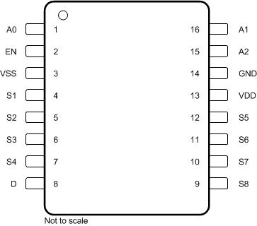
 Figure 6-1 PW Package, 16-Pin TSSOP
(Top View)
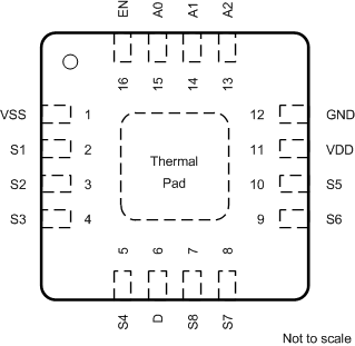
 Figure 6-2 RUM Package 16-Pin WQFN
(Top View)
Figure 6-2 RUM Package 16-Pin WQFN
(Top View)Table 6-1 Pin Functions:
TMUX8108
| PIN | TYPE(1) | DESCRIPTION | ||
|---|---|---|---|---|
| NAME | TSSOP | WQFN | ||
| A0 | 1 | 15 | I | Logic control input address 0 (A0). |
| EN | 2 | 16 | I | Active high digital enable (EN) pin. The device is disabled and all switches become high impedance when the pin is low. When the pin is high, the Ax logic inputs determine individual switch states. |
| VSS | 3 | 1 | P | Negative power supply. This pin is the most negative power-supply potential. In single-supply applications, this pin can be connected to ground. For reliable operation, connect a decoupling capacitor ranging from 0.1 µF to 10 µF between VSS and GND. |
| S1 | 4 | 2 | I/O | Source pin 1. Can be an input or output. |
| S2 | 5 | 3 | I/O | Source pin 2. Can be an input or output. |
| S3 | 6 | 4 | I/O | Source pin 3. Can be an input or output. |
| S4 | 7 | 5 | I/O | Source pin 4. Can be an input or output. |
| D | 8 | 6 | I/O | Drain pin. Can be an input or output. |
| S8 | 9 | 7 | I/O | Source pin 8. Can be an input or output. |
| S7 | 10 | 8 | I/O | Source pin 7. Can be an input or output. |
| S6 | 11 | 9 | I/O | Source pin 6. Can be an input or output. |
| S5 | 12 | 10 | I/O | Source pin 5. Can be an input or output. |
| VDD | 13 | 11 | P | Positive power supply. This pin is the most positive power-supply potential. For reliable operation, connect a decoupling capacitor ranging from 0.1 µF to 10 µF between VDD and GND. |
| GND | 14 | 12 | P | Ground (0 V) reference |
| A2 | 15 | 13 | I | Logic control input address 2 (A2). |
| A1 | 16 | 14 | I | Logic control input address 1 (A1). |
| Thermal Pad | — | The thermal pad is not connected internally. It is recommended to tie the pad to GND or VSS for the best performance. | ||
(1) I = input, O = output, I/O = input and output, P = power
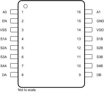
 Figure 6-3 PW Package, 16-Pin TSSOP
(Top View)
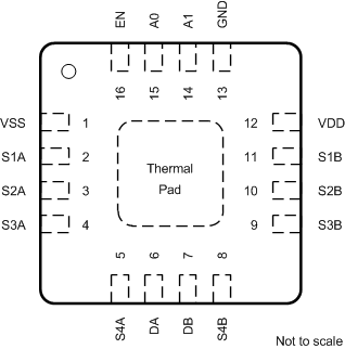
 Figure 6-4 RUM Package, 16-Pin WQFN
(Top View)
Figure 6-4 RUM Package, 16-Pin WQFN
(Top View)Table 6-2 Pin Functions:
TMUX8109
| PIN | TYPE(1) | DESCRIPTION | ||
|---|---|---|---|---|
| NAME | TSSOP | WQFN | ||
| A0 | 1 | 15 | I | Logic control input address 0 (A0). |
| EN | 2 | 16 | I | Active high digital enable (EN) pin. The device is disabled and all switches become high impedance when the pin is low. When the pin is high, the Ax logic inputs determine individual switch states. |
| VSS | 3 | 1 | P | Negative power supply. This pin is the most negative power-supply potential. In single-supply applications, this pin can be connected to ground. For reliable operation, connect a decoupling capacitor ranging from 0.1 µF to 10 µF between VSS and GND. |
| S1A | 4 | 2 | I/O | Source pin 1A. Can be an input or output. |
| S2A | 5 | 3 | I/O | Source pin 2A. Can be an input or output. |
| S3A | 6 | 4 | I/O | Source pin 3A. Can be an input or output. |
| S4A | 7 | 5 | I/O | Source pin 4A. Can be an input or output. |
| DA | 8 | 6 | I/O | Drain terminal A. Can be an input or output. |
| DB | 9 | 7 | I/O | Drain terminal B. Can be an input or output |
| S4B | 10 | 8 | I/O | Source pin 4B. Can be an input or output. |
| S3B | 11 | 9 | I/O | Source pin 3B. Can be an input or output. |
| S2B | 12 | 10 | I/O | Source pin 2B. Can be an input or output. |
| S1B | 13 | 11 | I/O | Source pin 1B. Can be an input or output. |
| VDD | 14 | 12 | P | Positive power supply. This pin is the most positive power-supply potential. For reliable operation, connect a decoupling capacitor ranging from 0.1 µF to 10 µF between VDD and GND. |
| GND | 15 | 13 | P | Ground (0 V) reference |
| A1 | 16 | 14 | I | Logic control input address 1 (A1). |
| Thermal Pad | — | The thermal pad is not connected internally. It is recommended to tie the pad to GND or VSS for the best performance. | ||
(1) I = input, O = output, I/O = input and output, P = power