ZHCSJG7D March 2019 – February 2024 TMUX1101 , TMUX1102
PRODUCTION DATA
- 1
- 1 特性
- 2 应用
- 3 说明
- 4 Device Comparison Table
- 5 Pin Configuration and Functions
-
6 Specifications
- 6.1 Absolute Maximum Ratings
- 6.2 ESD Ratings
- 6.3 Recommended Operating Conditions
- 6.4 Thermal Information
- 6.5 Electrical Characteristics (VDD = 5V ±10 %)
- 6.6 Electrical Characteristics (VDD = 3.3V ±10 %)
- 6.7 Electrical Characteristics (VDD = 1.8V ±10 %)
- 6.8 Electrical Characteristics (VDD = 1.2V ±10 %)
- 6.9 Typical Characteristics
- 7 Parameter Measurement Information
- 8 Detailed Description
- 9 Application and Implementation
- 10Device and Documentation Support
- 11Revision History
- 12Mechanical, Packaging, and Orderable Information
封装选项
请参考 PDF 数据表获取器件具体的封装图。
机械数据 (封装 | 引脚)
- DBV|5
- DCK|5
散热焊盘机械数据 (封装 | 引脚)
订购信息
8.3.6 Ultra-Low Charge Injection
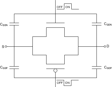
The TMUX110x devices have a transmission gate topology, as shown in Figure 8-2. Any mismatch in the stray capacitance associated with the NMOS and PMOS causes an output level change whenever the switch is opened or closed.
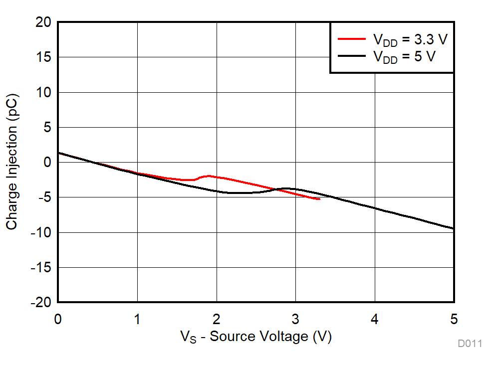
The TMUX110x devices have special charge-injection cancellation circuitry that reduces the source-to-drain charge injection to -1.5pC at VS = 1V as shown in Figure 8-3.
 Figure 8-2 Transmission Gate Topology
 Figure 8-3 Charge Injection vs Source Voltage