ZHCSJS9 May 2019 TLA2528
ADVANCE INFORMATION for pre-production products; subject to change without notice.
- 1 特性
- 2 应用
- 3 说明
- 4 修订历史记录
- 5 Pin Configuration and Functions
- 6 Specifications
-
7 Detailed Description
- 7.1 Overview
- 7.2 Functional Block Diagram
- 7.3 Feature Description
- 7.4 Device Functional Modes
- 7.5 Programming
- 7.6
TLA2528 Registers
- 7.6.1 SYSTEM_STATUS Register (Address = 0x0) [reset = 0x80]
- 7.6.2 GENERAL_CFG Register (Address = 0x1) [reset = 0x0]
- 7.6.3 DATA_CFG Register (Address = 0x2) [reset = 0x0]
- 7.6.4 OSR_CFG Register (Address = 0x3) [reset = 0x0]
- 7.6.5 OPMODE_CFG Register (Address = 0x4) [reset = 0x0]
- 7.6.6 PIN_CFG Register (Address = 0x5) [reset = 0x0]
- 7.6.7 GPIO_CFG Register (Address = 0x7) [reset = 0x0]
- 7.6.8 GPO_DRIVE_CFG Register (Address = 0x9) [reset = 0x0]
- 7.6.9 GPO_OUTPUT_VALUE Register (Address = 0xB) [reset = 0x0]
- 7.6.10 GPI_VALUE_LSB Register (Address = 0xD) [reset = 0x0]
- 7.6.11 SEQUENCE_CFG Register (Address = 0x10) [reset = 0x0]
- 7.6.12 CHANNEL_SEL Register (Address = 0x11) [reset = 0x0]
- 7.6.13 AUTO_SEQ_CHSEL Register (Address = 0x12) [reset = 0x0]
- 8 Application and Implementation
- 9 Power Supply Recommendations
- 10Layout
- 11器件和文档支持
- 12机械、封装和可订购信息
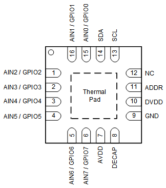
5 Pin Configuration and Functions
RTE Package
16-Pin WQFN
Top View

Pin Functions
| PIN | FUNCTION(1) | DESCRIPTION | |
|---|---|---|---|
| NAME | NO. | ||
| AIN0/GPIO0 | 15 | AI, DI, DO | Channel 0; configurable as either an analog input (default) or a general-purpose input/output (GPIO) |
| AIN1/GPIO1 | 16 | AI, DI, DO | Channel 1; configurable as either an analog input (default) or a GPIO |
| AIN2/GPIO2 | 1 | AI, DI, DO | Channel 2; configurable as either an analog input (default) or a GPIO |
| AIN3/GPIO3 | 2 | AI, DI, DO | Channel 3; configurable as either an analog input (default) or a GPIO |
| AIN4/GPIO4 | 3 | AI, DI, DO | Channel 4; configurable as either an analog input (default) or a GPIO |
| AIN5/GPIO5 | 4 | AI, DI, DO | Channel 5; configurable as either an analog input (default) or a GPIO |
| AIN6/GPIO6 | 5 | AI, DI, DO | Channel 6; configurable as either an analog input (default) or a GPIO |
| AIN7/GPIO7 | 6 | AI, DI, DO | Channel 7; configurable as either an analog input (default) or a GPIO |
| ADDR | 11 | AI | Input for selecting the device I2C address.
Connect a resistor to this pin from DECAP pin or GND to select one of the eight addresses. |
| AVDD | 7 | Supply | Analog supply input, also used as the reference voltage to the ADC; connect a 1-µF decoupling capacitor to GND |
| DECAP | 8 | Supply | Connect a decoupling capacitor to this pin for the internal power supply |
| DVDD | 10 | Supply | Digital I/O supply voltage; connect a 1-µF decoupling capacitor to GND |
| GND | 9 | Supply | Ground for the power supply; all analog and digital signals are referred to this pin voltage |
| NC | No connection | This pin must be left floating with no external connection | |
| SDA | 14 | DI, DO | Serial data input or output for the I2C interface |
| SCL | 13 | DI | Serial clock for the I2C interface |
(1) AI = analog input, DI = digital input, and DO = digital output.