SLOS358C September 2011 – April 2020 THS4531
PRODUCTION DATA.
- 1 Features
- 2 Applications
- 3 Description
- 4 Revision History
- 5 Packaging and Ordering Information
- 6 Electrical Specifications
- 7 Device Information
- 8 Table of Graphs
- 9 Typical Characteristics: VS = 2.7 V
- 10Typical Characteristics: VS = 5 V
-
11Application Information
- 11.1 Typical Characteristics Test Circuits
- 11.2
Application Circuits
- 11.2.1 Differential Input to Differential Output Amplifier
- 11.2.2 Single-Ended Input to Differential Output Amplifier
- 11.2.3 Differential Input to Single-Ended Output Amplifier
- 11.2.4 Input Common-Mode Voltage Range
- 11.2.5 Setting the Output Common-Mode Voltage
- 11.2.6 Single-Supply Operation
- 11.2.7 Low Power Applications and the Effects of Resistor Values on Bandwidth
- 11.2.8 Driving Capacitive Loads
- 11.2.9 Audio Performance
- 11.2.10 Audio On and Off Pop Performance
- 11.3 Audio ADC Driver Performance: THS4531 AND PCM4204 Combined Performance
- 11.4 SAR ADC Performance
- 11.5 EVM and Layout Recommendations
- 12Device and Documentation Support
- 13Mechanical, Packaging, and Orderable Information
封装选项
机械数据 (封装 | 引脚)
散热焊盘机械数据 (封装 | 引脚)
- RUN|10
订购信息
9 Typical Characteristics: VS = 2.7 V
Test conditions unless otherwise noted: VS+ = 2.7 V, VS– = 0 -, CM = open, VOUT = 2 Vpp, RF = 2 kΩ, RL = 2 kΩ differential, G = 1 V/V, single-ended input, differential output, input and output referenced to mid-supply unless otherwise noted.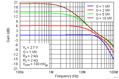 Figure 1. Small-Signal Frequency Response
 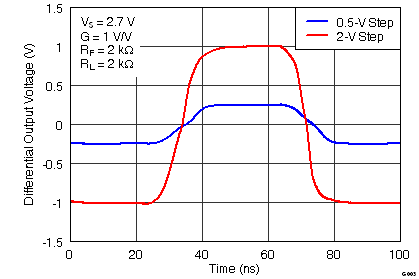 Figure 3. Large and Small-Signal Pulse Response
 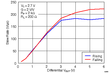 Figure 5. Differential Slew Rate vs VOUT Step
 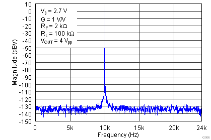 Figure 7. 10 kHz FFT On Audio Analyzer
 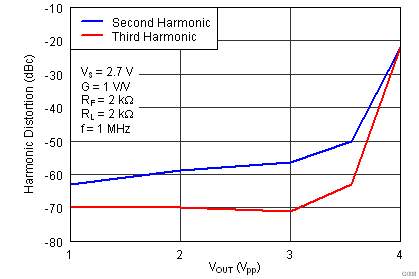 Figure 9. Harmonic Distortion vs Output Voltage at 1 MHz
 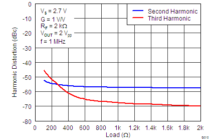 Figure 11. Harmonic Distortion vs Load at 1 MHz
 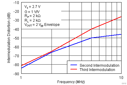 Figure 13. Two-Tone, 2nd and 3rd Order Intermodulation Distortion vs Frequency
 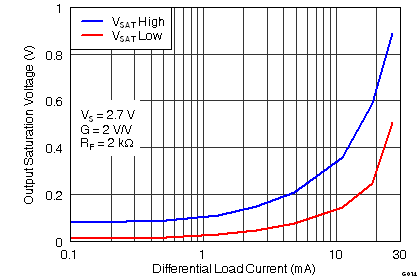 Figure 15. Single-Ended Output Saturation Voltage vs Load Current
 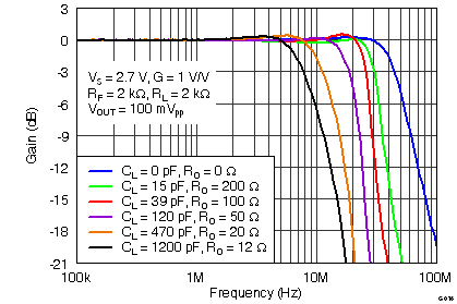 Figure 17. Frequency Response vs CLOAD
 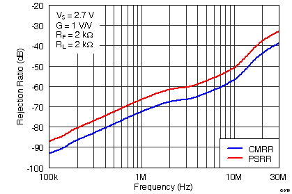 Figure 19. Rejection Ratio vs Frequency
 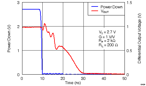 Figure 21. Turn-Off Time
 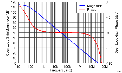 Figure 23. Main Amplifier Differential Open-Loop Gain and Phase vs Frequency
 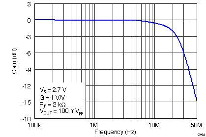 Figure 25. VOCM Small-Signal Frequency Response
 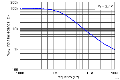 Figure 27. VOCM Input Impedance vs Frequency
 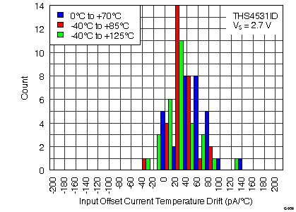 Figure 29. Input Offset Current Temperature Drift Histogram
 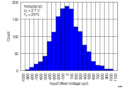 Figure 31. Input Offset Voltage Histogram
 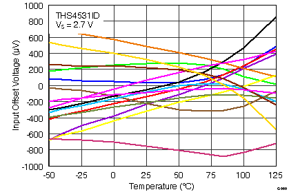 Figure 33. Input Offset Voltage vs Temperature
 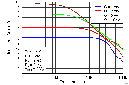 Figure 2. Large-Signal Frequency Response
 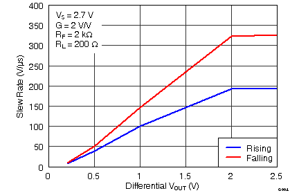 Figure 4. Single-Snded Slew Rate vs VOUT Step
 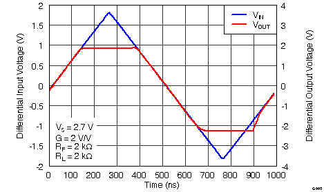 Figure 6. Overdrive Recovery
 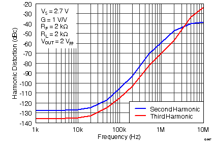 Figure 8. Harmonic Distortion vs Frequency
 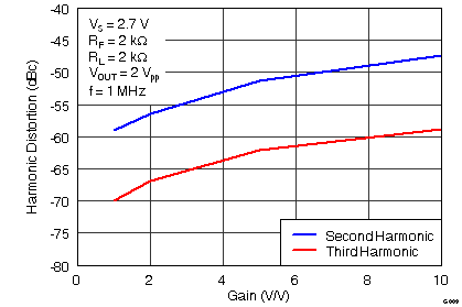 Figure 10. Harmonic Distortion vs GAIN at 1 MHz
 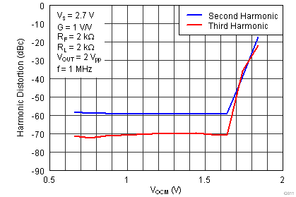 Figure 12. Harmonic Distortion vs VOCM at 1 MHz
 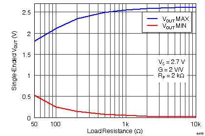 Figure 14. Single-Ended Output Voltage Swing vs Load Resistance
 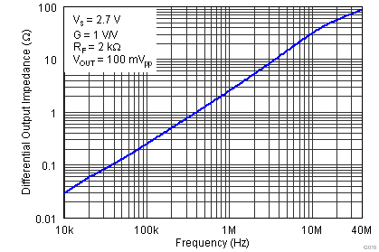 Figure 16. Main Amplifier Differential Output Impedance vs Frequency
 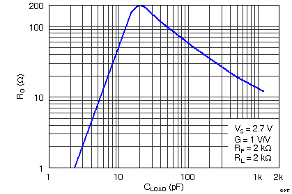 Figure 18. RO vs CLOAD
 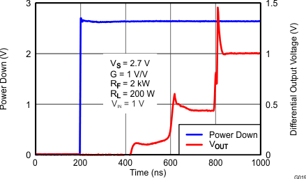 Figure 20. Turn-On Time
 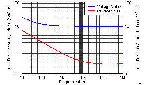 Figure 22. Input-referred Voltage Noise and Current Noise Spectral Density
 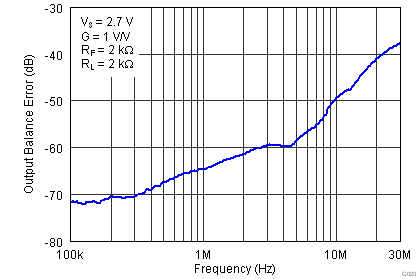 Figure 24. Output Balance Error vs Frequency
 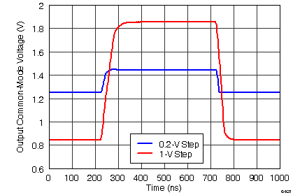 Figure 26. VOCM Large and Small-Signal Pulse Response
 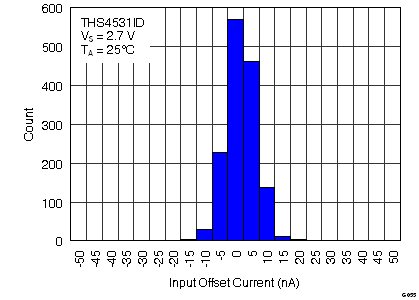 Figure 28. Input Offset Current Histogram
 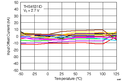 Figure 30. Input Offset Current vs Temperature
 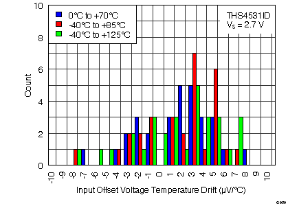 Figure 32. Input Offset Voltage Temperature Drift Histogram