ZHCSHX6C August 2017 – February 2023 THS3491
PRODUCTION DATA
- 1 特性
- 2 应用
- 3 说明
- 4 Revision History
- 5 Device Comparison Table
- 6 Pin Configuration and Functions
- 7 Bare Die Information
- 8 Specifications
- 9 Detailed Description
- 10Application and Implementation
- 11Device and Documentation Support
- 12Mechanical, Packaging, and Orderable Information
封装选项
机械数据 (封装 | 引脚)
散热焊盘机械数据 (封装 | 引脚)
订购信息
10.4.1.1.1 PowerPAD™ Integrated Circuit Package Layout Considerations
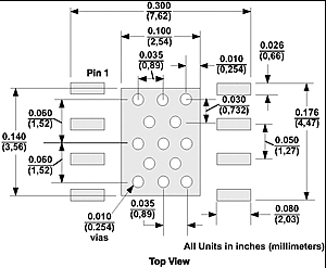
The DDA package top-side etch and via pattern is shown in Figure 10-11.
 Figure 10-11 DDA PowerPAD™ Integrated Circuit Package PCB Etch and Via Pattern
- Use etch for the leads and the thermal pad.
- Place 13 vias in the thermal pad area. These vias must be 0.01 inch (0.254 mm) in diameter. Keep the vias small so that solder wicking through the vias is not a problem during reflow.
- Additional vias may be placed anywhere along the thermal plane outside of the thermal pad area, and help dissipate the heat generated by the THS3491 device. These additional vias may be larger than the 0.01-inch (0.254 mm) diameter vias directly under the thermal pad because they are not in the area that requires soldering. As a result, wicking is not a problem.
- Connect all vias to the internal ground plane. The PowerPAD integrated circuit package is electrically isolated from the silicon and all leads. Connecting the PowerPAD integrated circuit package to any potential voltage such as –VS is acceptable because there is no electrical connection to the silicon.
- When connecting these vias to the ground plane, do not use the typical web or spoke through connection methodology. Web and spoke connections have a high thermal resistance that slows the heat transfer during soldering . Avoiding these connection methods makes the soldering of vias that have plane connections easier. In this application, however, low thermal resistance is desired for the most efficient heat transfer. Therefore, the vias under the THS3491 PowerPAD integrated circuit package must connect to the internal ground plane with a complete connection around the entire circumference of the plated-through hole.
- The top-side solder mask must leave the pins of the package and the thermal pad area with the 13 vias exposed.
- Apply solder paste to the exposed thermal pad area and all of the device pins.
- With these preparatory steps in place, the device is placed in position and run through the solder reflow operation as any standard surface-mount component. This results in a device that is properly installed.