ZHCSHX6C August 2017 – February 2023 THS3491
PRODUCTION DATA
- 1 特性
- 2 应用
- 3 说明
- 4 Revision History
- 5 Device Comparison Table
- 6 Pin Configuration and Functions
- 7 Bare Die Information
- 8 Specifications
- 9 Detailed Description
- 10Application and Implementation
- 11Device and Documentation Support
- 12Mechanical, Packaging, and Orderable Information
封装选项
机械数据 (封装 | 引脚)
散热焊盘机械数据 (封装 | 引脚)
订购信息
10.1.1 Driving Capacitive Loads
Applications such as power JFET and MOSFET (power FET) drivers are highly capacitive and cause stability problems for high-speed amplifiers.
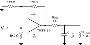
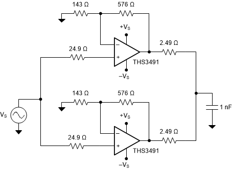
Figure 10-1 and Figure 10-2 show recommended methods for driving capacitive loads. The basic idea is to use a resistor or ferrite chip to isolate the phase shift at high frequency caused by the capacitive load from the amplifier feedback path. The output impedance of the amplifier in conjunction with CLOAD introduces a pole in the open-loop transimpedance gain response and if the pole is at a frequency lower than the non-dominant pole of the amplifier, then this results in a reduced loop gain and a reduced phase margin. The isolation resistor introduces a zero in the response, which counteracts the effect of the pole. The location of the zero is dependent on the values of RISO and CLOAD. Figure 8-5 shows examples of the recommended RISO values to achieve flat frequency response while driving certain capacitive loads. See Effect of Parasitic Capacitance in Op Amp Circuits for a detailed analysis of selecting isolation resistor values while driving capacitive loads.
 Figure 10-1 Driving a Large Capacitive Load Using an Output Series Isolation Resistor
Placing a small series resistor (RISO) between the output of the amplifier and the capacitive load as Figure 10-1 shows is a simple way to isolate the load capacitance.
Figure 10-2 shows two amplifiers in parallel to double the output drive current in order to drive larger capacitive loads. This technique is used when more output current is required to charge and discharge the load faster, such as driving large FET transistors.
 Figure 10-2 Driving a Large Capacitive Load Using Two Parallel Amplifier Channels
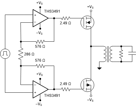
Figure 10-3 shows a push-pull FET driver circuit commonly used in ultrasound applications with isolation resistors to isolate the gate capacitance from the amplifier.
 Figure 10-3 Power FET Drive Circuit