ZHCSCU3C January 2014 – September 2019 TCA5013
PRODUCTION DATA.
- 1 特性
- 2 应用
- 3 说明
- 4 修订历史记录
- 5 Pin Configuration and Functions
-
6 Specifications
- 6.1 Absolute Maximum Ratings
- 6.2 Handling Ratings
- 6.3 Recommended Operating Conditions
- 6.4 Thermal Information
- 6.5 Electrical Characteristics—Power Supply and ESD
- 6.6 Electrical Characteristics—Card VCC
- 6.7 Electrical Characteristics—Card RST
- 6.8 Electrical Characteristics—Card CLK
- 6.9 Electrical Characteristics—Card Interface IO, C4 and C8
- 6.10 Electrical Characteristics—PRES
- 6.11 Electrical Characteristics—IOMC1 and IOMC2
- 6.12 Electrical Characteristics—CLKIN1 and CLKIN2
- 6.13 Electrical Characteristics—A0 and SHDN
- 6.14 Electrical Characteristics—INT
- 6.15 Electrical Characteristics—GPIO
- 6.16 Electrical Characteristics—SDA and SCL
- 6.17 Electrical Characteristics—Fault Condition Detection
- 6.18 I2C Interface Timing Requirements
- 6.19 I2C Interface Timing Characteristics
- 6.20 Synchronous Type 1 Card Activation Timing Characteristics
- 6.21 Synchronous Type 2 Card Activation Timing Characteristics
- 6.22 Card Deactivation Timing Characteristics
- 6.23 Typical Characteristics
- 7 Parameter Measurement Information
-
8 Detailed Description
- 8.1 Overview
- 8.2 Functional Block Diagram
- 8.3 Feature Description
- 8.4 Device Functional Modes
- 8.5 Programming
- 8.6 Register Maps
- 9 Application and Implementation
- 10Power Supply Recommendations
- 11Layout
- 12器件和文档支持
- 13机械、封装和可订购信息
8.4.5 User Card Insertion / Removal Detection
User card interface module in the TCA5013 has a PRES pin that is used to detect the presence of a card in that interface. In normal application the signal is connected to a switch that opens or closes when a card is inserted. Whenever a transition is seen on the PRES pin, the PRESL bit (Reg 0x00, bit 2) will be set and INT pin is asserted. Because this transition is associated with a mechanical switch, there is an internal debounce of ~20 ms before the PRESL bit is set and the INT is asserted. If the device sees a transition on the PRESL pin when the card interface is active, the device initiates a card deactivation sequence (see Deactivation Sequence). TCA5013 is capable of detecting card insertion even when it is in shutdown mode (see Shutdown Mode).
In addition to the PRESL_UC bit mentioned above, there is also a PRES_UC bit (Reg 0x00, bit 2), which indicates to the host whether or not a card is present in the user card slot. In order to accommodate different card cage topologies, the TCA5013 can be configured to detect card presence with a low to high or high to low, transition on the PRES pin. The CARD_DETECT_UC bit (Reg 0x01, bit 2) is used to configure the device for different card detection topologies. If CARD_DETECT_UC = 0 indicates to the TCA5013 that when a card is inserted in the slot, the PRES pin shall be low. CARD_DETECT_UC = 1 indicates to the host that when a card is inserted in the slot the PRES pin shall be high. The status of the PRES_UC bit is based on the status of the PRES pin and the CARD_DETECT_UC bit. The truth table in Table 1 shows the PRES_UC bit status based on the CARD_DETECT_UC bit and the PRES pin. When coming out of power off mode (see Power Off Mode) or shutdown mode (see Shutdown Mode) the CARD_DETECT_UC = 0. If there is a state transition on the PRES pin when the device is in shutdown mode, the INT pin asserted (after the 20 ms debounce).
Table 5. Truth Table Defining Status of PRES Bit
| CARD DETECT BIT | PRES PIN | PRES BIT |
|---|---|---|
| 0 | 0 | 1 |
| 0 | 1 | 0 |
| 1 | 0 | 0 |
| 1 | 1 | 1 |
Figure 9 to Figure 14 show timing waveforms of device power up and coming out of shutdown with and without a card inserted in the system. In below figures’ low to high PRES topology’ means that a high level on the PRES pin indicates a card is present. In below figures high to low PRES topology’ means that a low level on the PRES pin indicates a card is present. The below figures also show operation of INT pin and interrupt status register. For detailed description of the interrupt operation, refer to Interrupt Operation section.
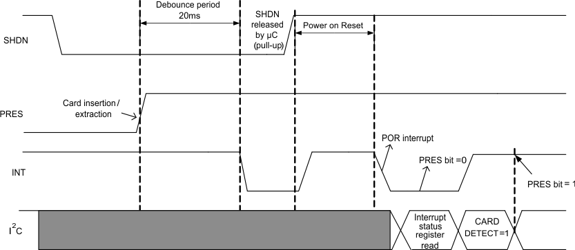 Figure 9. Card detection in shutdown mode - Low to High PRES Topology
 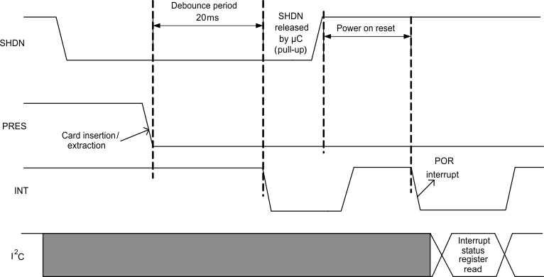 Figure 10. Card detection in shutdown mode - High to Low PRES Topology
 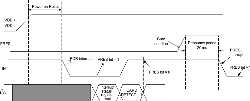 Figure 11. Device power up without card inserted in system - Low to High PRES Topology
 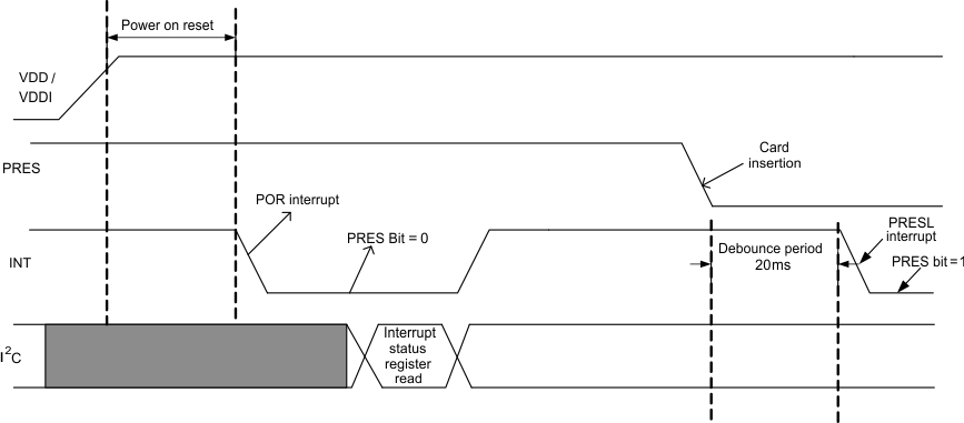 Figure 12. Device power up without card inserted in system - High to Low PRES Topology
 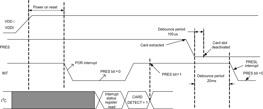 Figure 13. Device Power Up With Card Inserted in System - Low to High PRES Topology
 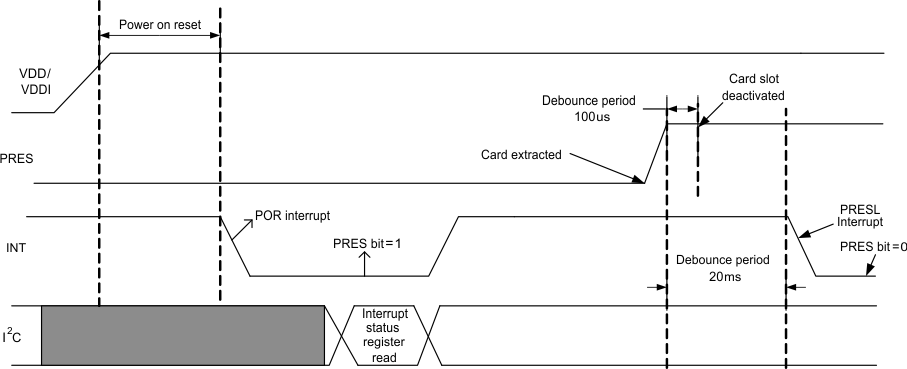 Figure 14. Device Power up with Card Inserted In System - High to Low PRES Topology