ZHCSBQ4B September 2013 – September 2014 SN65LVDS822
PRODUCTION DATA.
- 1 特性
- 2 应用范围
- 3 说明
- 4 修订历史记录
- 5 说明(继续)
- 6 Pin Configuration and Functions
- 7 Specifications
- 8 Parameter Measurement Information
- 9 Detailed Description
- 10Application and Implementation
- 11Power Supply Recommendations
- 12Layout
- 13器件和文档支持
- 14机械封装和可订购信息
7 Specifications
7.1 Absolute Maximum Ratings(1)
| MIN | MAX | UNIT | ||
|---|---|---|---|---|
| Supply voltage range(2), VDD , VDDIO | –0.3 | 4 | V | |
| Voltage range at any input terminal | When VDDIO > 0 V | –0.5 | 4 | V |
| Voltage range at any output terminal | When VDDIO ≤ 0 V | –0.5 | VDDIO + 0.7 | |
| Maximum junction temperature, TJ | 125 | °C | ||
(1) Stresses beyond those listed under Absolute Maximum Ratings may cause permanent damage to the device. These are stress ratings only and functional operation of the device at these or any other conditions beyond those indicated under Recommended Operating Conditions is not implied. Exposure to absolute maximum-rated conditions for extended periods may affect device reliability.
(2) All voltage values are with respect to the GND terminals
7.2 Handling Ratings
| MIN | MAX | UNIT | |||
|---|---|---|---|---|---|
| Tstg | Storage temperature range | –65 | 150 | °C | |
| V(ESD) | Electrostatic discharge | Human body model(1) (all pins) | –3 | 3 | V |
| Charged device model(2) (all pins) | –1.5 | 1.5 | |||
(1) In accordance with JEDEC Standard 22, Test Method A114-B
(2) In accordance with JEDEC Standard 22, Test Method C101
7.3 Recommended Operating Conditions
| TEST CONDITIONS | MIN | TYP | MAX | UNIT | |||
|---|---|---|---|---|---|---|---|
| VDD | Main power supply | 3 | 3.3 | 3.6 | V | ||
| VDDIO | Power supply for CMOS outputs | 1.65 | 3.6 | V | |||
| VNOISE | Power supply noise (peak-to-peak) |
fNOISE < 1 MHz | 100 | mV | |||
| fNOISE > 1 MHz | 50 | ||||||
| TA | Operating free-air temperature | –40 | 85 | °C | |||
| TC | Case temperature | 98 | °C | ||||
| LVDS CLOCK (CLKP, CLKN) | |||||||
| fCLK | LVDS clock frequency | MODE14 = Low | 4 | 54 | MHz | ||
| MODE14 = High | 4 | 27 | |||||
| Standby Mode | 0.5 | ||||||
| tDC | LVDS clock duty cycle | MODE14 = Low | 57% | ||||
| MODE14 = High | 50% | ||||||
| LVDS INPUTS (A0P, A0N, A1P, A1N, A2P, A2N, A3P, A3N, CLKP, CLKN) | |||||||
| |VID| | Input differential voltage(1) | |VAxP – VAxN| and |VCLKP-VCLKN| | 90 | 600 | mV | ||
| ΔVID | Input differential voltage variation between lanes | –10% | 10% | ||||
| VCM | Input common mode voltage(1) | |VID|/2 | 2.4 - |VID|/2 | V | |||
| ΔVCM | Input common mode voltage variation between lanes | –100 | 100 | mV | |||
| tR/F(VID) | LVDS VID rise/fall time(2) | MODE14 = Low | fCLK = 4 MHz to 14 MHz | 3 | ns | ||
| fCLK = 14 MHz to 22 MHz | 2 | ||||||
| fCLK = 22 MHz to 30 MHz | 1.5 | ||||||
| fCLK = 30 MHz to 54 MHz | 1 | ||||||
| MODE14 = High | fCLK = 4 MHz to 7 MHz | 3 | |||||
| fCLK = 7 MHz to 11 MHz | 2 | ||||||
| fCLK = 11 MHz to 15 MHz | 1.5 | ||||||
| fCLK = 15 MHz to 27 MHz | 1 | ||||||
| CMOS OUTPUTS (D[26:0], CLKOUT) | |||||||
| CL | Capacitive load on the outputs | 10 | pF | ||||
(1) See Figure 1.
(2) See Figure 6. Defined from 20% to 80% of the differential voltage transition. Faster edge rates are generally preferred, as they provide more timing margin.
7.4 Thermal Information
| THERMAL METRIC(1) | SN65LVDS822 | UNIT | |
|---|---|---|---|
| RGZ | |||
| 48 PINS | |||
| θJA | Junction-to-ambient thermal resistance(2) | 30.1 | °C/W |
| θJCtop | Junction-to-case (top) thermal resistance(3) | 18.1 | |
| θJB | Junction-to-board thermal resistance(4) | 6.9 | |
| ψJT | Junction-to-top characterization parameter(5) | 0.2 | |
| ψJB | Junction-to-board characterization parameter(6) | 6.9 | |
| θJCbot | Junction-to-case (bottom) thermal resistance(7) | 0.7 | |
(1) For more information about traditional and new thermal metrics, see the IC Package Thermal Metrics application report, SPRA953.
(2) The junction-to-ambient thermal resistance under natural convection is obtained in a simulation on a JEDEC-standard, high-K board, as specified in JESD51-7, in an environment described in JESD51-2a.
(3) The junction-to-case (top) thermal resistance is obtained by simulating a cold plate test on the package top. No specific JEDEC-standard test exists, but a close description can be found in the ANSI SEMI standard G30-88.
(4) The junction-to-board thermal resistance is obtained by simulating in an environment with a ring cold plate fixture to control the PCB temperature, as described in JESD51-8.
(5) The junction-to-top characterization parameter, ψJT, estimates the junction temperature of a device in a real system and is extracted from the simulation data for obtaining θJA, using a procedure described in JESD51-2a (sections 6 and 7).
(6) The junction-to-board characterization parameter, ψJB, estimates the junction temperature of a device in a real system and is extracted from the simulation data for obtaining θJA , using a procedure described in JESD51-2a (sections 6 and 7).
(7) The junction-to-case (bottom) thermal resistance is obtained by simulating a cold plate test on the exposed (power) pad. No specific JEDEC standard test exists, but a close description can be found in the ANSI SEMI standard G30-88.
7.5 DC Electrical Characteristics
over operating free-air temperature range (unless otherwise noted)| PARAMETER | TEST CONDITIONS | MIN | TYP(1) | MAX | UNIT | |
|---|---|---|---|---|---|---|
| LVDS INPUTS (A0P, A0N, A1P, A1N, A2P, A2N, A3P, A3N, CLKP, CLKN) | ||||||
| RID | Differential input termination resistance(1) | SWAP = Low or High | 80 | 132 | Ω | |
| CID | Differential input capacitance | Measured across differential pairs | 1 | pF | ||
| RPU | Pull-up resistor for standby detection | Measured from each input to VDD | 90 | kΩ | ||
| |II| | Input leakage current | VDD = 3.6 V; RID disconnected; One P/N terminal is swept from 0 V to 2.4 V while the other is 1.2 V | 70 | µA | ||
| CMOS INPUTS (SWAP, MODE14, CLKPOL, SHTDN#, SLEW) | ||||||
| CIN | Input capacitance for CMOS inputs | 2 | pF | |||
| VIK | Input clamp voltage | II = -18 mA | –1.2 | V | ||
| VIH | High-level input voltage | 0.8 x VDD | V | |||
| VIL | Low-level input voltage | 0.2 x VDD | V | |||
| 3-STATE CMOS INPUTS (SWAP, CLKPOL, SLEW) | ||||||
| VF | Floating voltage | VIN = High impedance | VDD/2 | V | ||
| IIH | High-level input current (through pull-down) | VIN = 3.6 V | 36 | µA | ||
| IIL | Low-level input current (through pull-up) | VIN = GND, VDD = 3.6 V | -36 | µA | ||
| 2-STATE CMOS INPUTS (MODE14, SHTDN#) | ||||||
| IIH | High-level input current (through pull-down) | VIN = 3.6 V | 20 | µA | ||
| IIL | Low-level input current | VIN = GND | 0 | µA | ||
| CMOS OUTPUTS (D[26:0], CLKOUT) | ||||||
| VOH | High-level output voltage | SLEW = Low; IOH = -250 µA | 0.8 x VDDIO | VDDIO | V | |
| SLEW = Floating; IOH = -500 µA | 0.8 x VDDIO | VDDIO | ||||
| SLEW = High; IOH = -1.33 mA | 0.8 x VDDIO | VDDIO | ||||
| VOL | Low-level output voltage | SLEW = Low; IOL = 250 µA | 0 | 0.5 | V | |
| SLEW = Floating; IOL = 500 µA | 0 | 0.5 | ||||
| SLEW = High; IOL = 1.33 mA | 0 | 0.5 | ||||
(1) When VDD = 0 V, the connection of RID is unknown.
7.6 Power Supply Characteristics
over recommended operating conditions (unless otherwise noted)| PARAMETER | TEST CONDITIONS(1)(2) | TYP | MAX(1) | UNIT | |||
|---|---|---|---|---|---|---|---|
| IDD | Total average supply current of VDD and VDDIO | Grayscale pattern; outputs terminated with 10 pF; MODE14 = Low, VDD = 3.3 V, VDDIO = 1.8 V | SLEW = Low; fCLK = 10 MHz | 24.6 | mA | ||
| Grayscale pattern; outputs terminated with 10pF; MODE14 = Low, VDD = VDDIO = 3.3 V | SLEW = Low; fCLK = 10 MHz | 25.7 | mA | ||||
| SLEW = Float; fCLK = 20 MHz | 30.9 | ||||||
| SLEW = High; fCLK = 54 MHz | 51.5 | ||||||
| 1010 pattern; outputs terminated with 10 pF; MODE14 = Low, VDD = VDDIO = 3.6 V | SLEW = Float; fCLK = 20 MHz | 48.2 | 59 | mA | |||
| SLEW = High; fCLK = 54 MHz | 101.7 | 124 | |||||
| Standby Mode | LVDS inputs are open; CMOS inputs held static; Outputs terminated with 10 pF | fCLK < 500 kHz; VCM-CLKP/N ≤ 0.80 x VDD |
4 | 7 | mA | ||
| VCM-CLKP/N > 0.95 x VDD | 75 | 130 | µA | ||||
| Shutdown Mode | SHTDN# = Low | 4 | 20 | ||||
| PD | Power Dissipation | Grayscale pattern; outputs terminated with 10 pF; MODE14 = Low, VDD = 3.3 V, VDDIO = 1.8 V | SLEW = Low; fCLK = 10 MHz | 83 | mW | ||
| 1010 pattern; outputs terminated with 10 pF; MODE14 = Low, VDD = VDDIO = 3.6 V | SLEW = High; fCLK = 54 MHz | 366 | 446 | ||||
(2) Standby Mode can be entered in two ways: fCLK = zero to 500 kHz, or a high VCM on the LVDS clock. If the LVDS transmitter device disables its clock driver to a high-impedance state, the SN65LVDS822’s integrated RPU will pull VCM high for the lower-power Standby state.
7.7 Switching Characteristics
over recommended operating conditions (unless otherwise noted)| PARAMETER | TEST CONDITIONS | MIN | TYP(1) | MAX | UNIT | ||
|---|---|---|---|---|---|---|---|
| INPUT TO OUTPUT RESPONSE TIME | |||||||
| tPD | Propagation delay of data | Measured from CLK input to CLKOUT | 2.4/fCLK | s | |||
| tPWRUP | Enable time, exiting Shutdown | From Shutdown Mode, time from SHTDN# pulled High to valid output data (see Figure 9) | 2 | ms | |||
| tWAKE | Enable time, exiting Standby | From Standby Mode, time from when CLK input starts switching to valid output data | 2 | ms | |||
| tPWRDN | Disable time, entering Shutdown | From Active Mode, time from SHTDN# pulled Low until all outputs are static-Low | 11 | µs | |||
| tSTANDBY | Disable time, entering Standby | From Active Mode, time from CLK input stopping until all outputs are static-Low | 3 | µs | |||
| fBW | PLL bandwidth(1) | Tested from CLK input to CLKOUT | 6% x fCLK | Hz | |||
| LVDS INPUTS (A0P, A0N, A1P, A1N, A2P, A2N, A3P, A3N, CLKP, CLKN) | |||||||
| tRSKM | Receiver input skew margin(2)(3)(4) | tR/F(VID) = 600 ps VID = 90 mV See Figure 2 |
MODE14 = Low | 1/(14 x fCLK) – 620E-12 | s | ||
| MODE14 = High | 1/(28 x fCLK) – 620E-12 | ||||||
| tSU1 | LVDS data setup time required before internal clock edge | 620 | ps | ||||
| tH1 | LVDS data hold time required after internal clock edge | 620 | ps | ||||
| CMOS OUTPUTS (D[26:0], CLKOUT) | |||||||
| tDCYC | Duty cycle of CLKOUT | MODE14 = Low | CLKPOL = Low | 43% | |||
| CLKPOL = High | 57% | ||||||
| MODE14 = High | 50% | ||||||
| tR/F | CMOS output rise and fall time (20% to 80%) | CL = 10 pF | SLEW = Low | 10 | 15 | 20 | ns |
| SLEW = Floating | 5 | 7.5 | 10 | ||||
| SLEW = High | 1.3 | 2.1 | 3 | ||||
| tSU2 | Setup time available for the downstream receiver(5) | MODE14 = Low; CL = 10 pF | SLEW = Low | 0.38/fCLK – 2.2E-9 | s | ||
| SLEW = Floating | 0.38/fCLK – 1.2E-9 | ||||||
| SLEW = High | 0.38/fCLK – 0.7E-9 | ||||||
| MODE14 = High; CL = 10 pF | SLEW = Low | 0.45/fCLK – 2.5E-9 | |||||
| SLEW = Floating | 0.45/fCLK – 1.5E-9 | ||||||
| SLEW = High | 0.45/fCLK – 1E-9 | ||||||
| tH2 | Hold time available for the downstream receiver(5) | MODE14 = Low; CL = 10 pF | SLEW = Low | 0.52/fCLK – 18.2E-9 | s | ||
| SLEW = Floating | 0.52/fCLK – 9.2E-9 | ||||||
| SLEW = High | 0.52/fCLK – 3.7E-9 | ||||||
| MODE14 = High; CL = 10 pF | SLEW = Low | 0.45/fCLK – 18.5E-9 | |||||
| SLEW = Floating | 0.45/fCLK – 9.5E-9 | ||||||
| SLEW = High | 0.45/fCLK – 4E-9 | ||||||
(1) The PLL bandwidth describes the typical highest modulation frequency that can be tracked. If the LVDS transmitter device generates a spread spectrum, the LVDS clock and data must stay synchronized throughout modulation. The SN65LVDS822 will track and pass through modulation, and the downstream CMOS receiver must be able to track it.
(2) Receiver Input Skew Margin (tRSKM) is the timing margin available for transmitter output pulse position (tPPOS), interconnect skew, and interconnect inter-symbol interference. tRSKM represents the reminder of the serial bit time not taken up by the receiver strobe uncertainty. The tRSKM assumes a bit error rate better than 10-12.
(3) tRSKM is indirectly proportional to: internal setup and hold time uncertainty, ISI, duty cycle distortion from the front end receiver, skew mismatch between LVDS clock and data, and PLL cycle-to-cycle jitter.
(4) LVDS input timing defined here is based on a simulated statistical analysis across process, voltage, and temperature ranges.
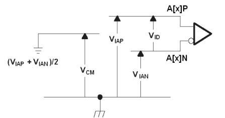 Figure 1. FlatLink™ Input Voltage Definitions
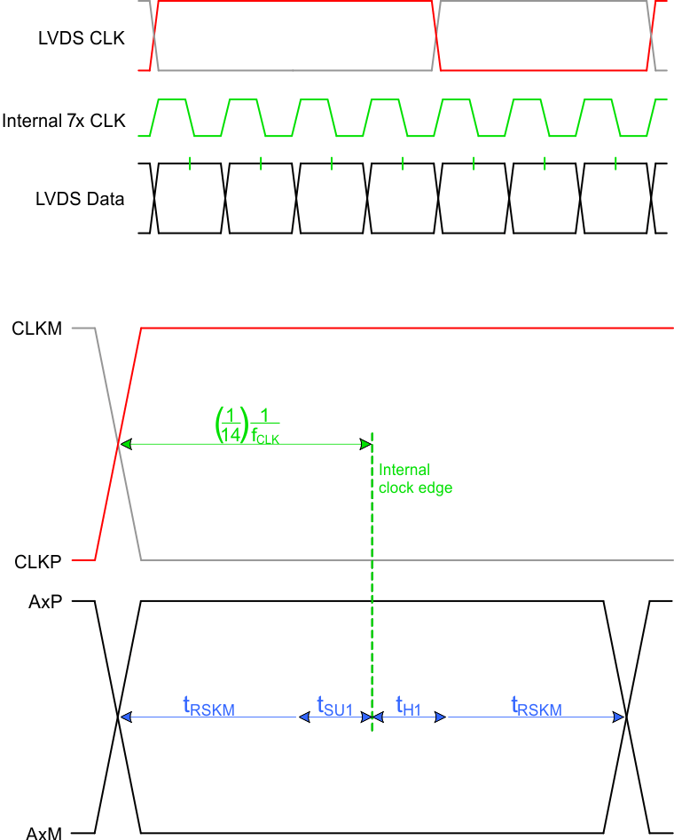 Figure 2. LVDS Input Timing (MODE14 = Low)
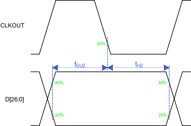 Figure 3. CMOS Output Timing (CLKPOL = Low)
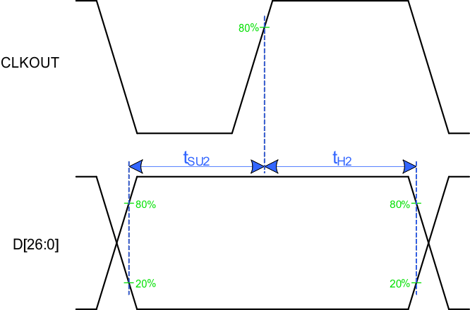 Figure 4. CMOS Output Timing (CLKPOL = High)
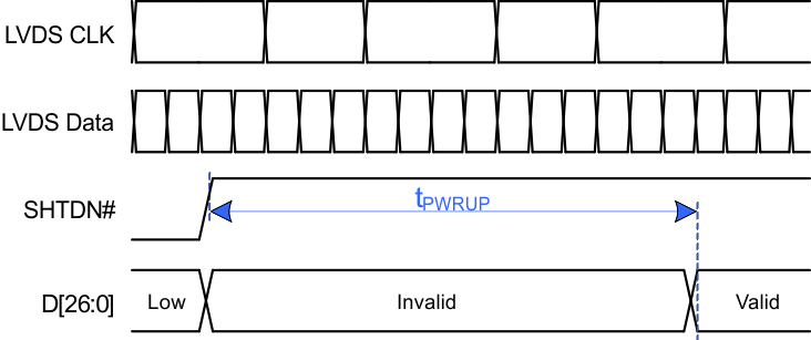 Figure 5. Time to Exit Shutdown Mode
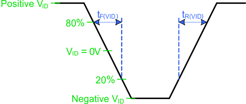 Figure 6. LVDS Rise/Fall Time (Differential Voltage)
7.8 Typical Characteristics
space
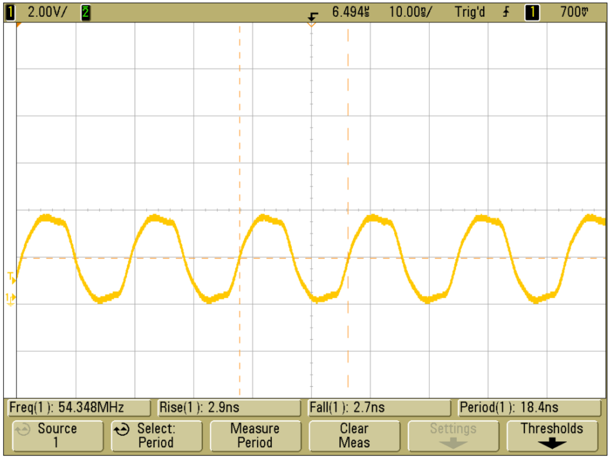
Figure 7. Output Rise & Fall times - SLEW = High
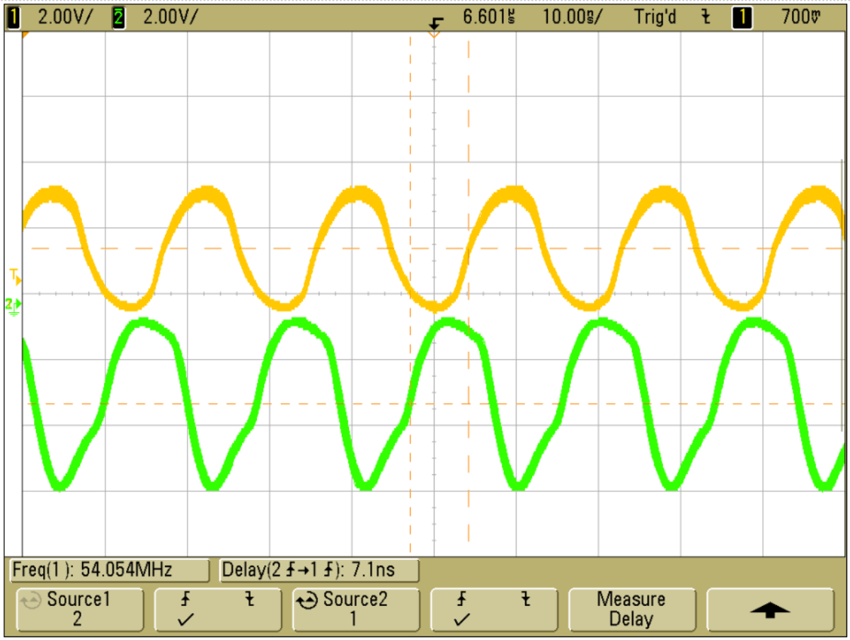
Input: channel 2 (green), Output: channel 1 (yellow)
Figure 8. Total Output Delay