ZHCSBQ4B September 2013 – September 2014 SN65LVDS822
PRODUCTION DATA.
- 1 特性
- 2 应用范围
- 3 说明
- 4 修订历史记录
- 5 说明(继续)
- 6 Pin Configuration and Functions
- 7 Specifications
- 8 Parameter Measurement Information
- 9 Detailed Description
- 10Application and Implementation
- 11Power Supply Recommendations
- 12Layout
- 13器件和文档支持
- 14机械封装和可订购信息
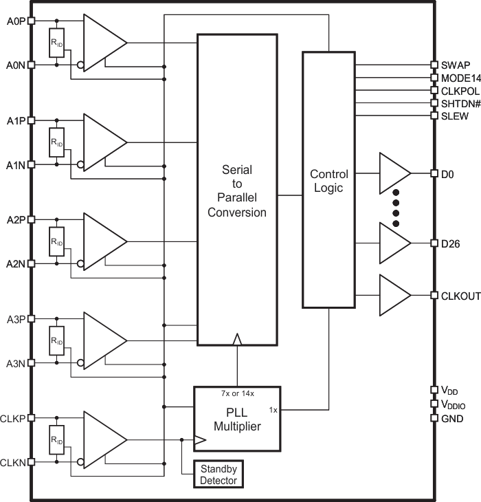
9 Detailed Description
9.1 Overview
The SN65LVDS822 implements five low-voltage differential signal (LVDS) line receivers: 4 data lanes and 1 clock lane. The clock is internally multiplied by 7 or 14 (depending on pin MODE14), and used for sampling LVDS data. The device operates in either 4-lane 7x mode, or 2-lane 14x mode. Each input lane contains a shift register that converts serial data to parallel. 27 total bits per clock period are deserialized and presented on the CMOS output bus, along with a clock that uses either rising- or falling-edge alignment.
9.2 Functional Block Diagram
9.3 Feature Description
9.3.1 Unused LVDS Data Lanes
When MODE14 = Low and fewer than 4 data lanes are used, or when MODE14 = High and only 1 data lane is used, it’s recommended that the unused lanes are biased with a constant differential voltage. This prevents high-frequency noise from toggling the unused receiver, which injects noise into the device. This is not a hard requirement, but it’s standard best-practice, and the amount of noise varies system-to-system.
Two implementations are shown below, depending on whether the internal termination RID is connected. A reasonable choice for R1 and R2 is 5kΩ, which produce a nominal VID of 34 mV and 0.3 mA of static current. Smaller resistors increase VID and noise floor margin, as well as static current.
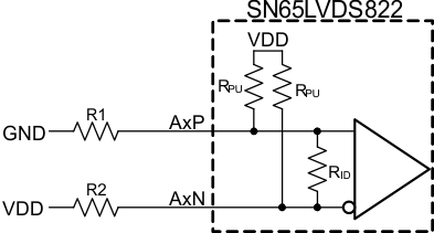 Figure 12. Bias When RID is Connected
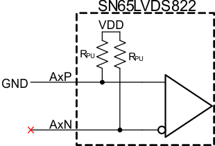 Figure 13. Bias When RID is Disconnected
9.3.2 Tying CMOS Inputs With Resistors
The IIH/IIL specifications indicate that 2-state CMOS input pins have an internal pull-down that’s a minimum size of 180 kΩ, and 3-state CMOS input pins have an internal pull-up and pull-down that are a minimum size of
100 kΩ.
 Figure 14. 2-State CMOS Input
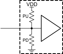 Figure 15. 3-State CMOS Input
CMOS inputs may be directly connected to VDD or GND, or tied through a resistor. Using a resistor creates a voltage divider network, so it’s important to use a small enough resistor to satisfy VIH/VIL at the pin, and to have voltage margin for system noise. When using a resistor, 5 kΩ or smaller is recommended. Of course, 3-state inputs may be left unconnected to select their floating pin state.
9.4 Device Functional Modes
9.4.1 Active Modes
9.4.1.1 4-Lanes 7-Bit Mode
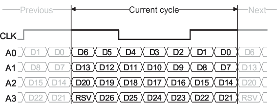 Figure 16. Data Bits Within the LVDS Stream (MODE14 = Low)
9.4.1.2 2-Lanes 14-Bit Mode
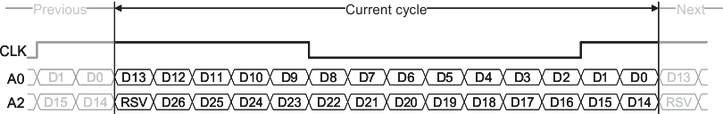 Figure 17. Data Bits Within the LVDS Stream (MODE14 = High)
9.4.2 Low-Power Modes
9.4.2.1 Standby Mode
In order to decrease the power consumption, the SN65LVDS822 automatically enters to standby when the LVDS clock is inactive.
9.4.2.2 Shutdown Mode
This is the lower-power mode, and the SN65LVDS822 enters to this mode only when the SHTDN# terminal is tied to low.
NOTE
In both low-power modes, all CMOS outputs drive low. All input pins have failsafe protection that prevents damage from occurring before power supply voltages are high and stable.