ZHCSBQ4B September 2013 – September 2014 SN65LVDS822
PRODUCTION DATA.
- 1 特性
- 2 应用范围
- 3 说明
- 4 修订历史记录
- 5 说明(继续)
- 6 Pin Configuration and Functions
- 7 Specifications
- 8 Parameter Measurement Information
- 9 Detailed Description
- 10Application and Implementation
- 11Power Supply Recommendations
- 12Layout
- 13器件和文档支持
- 14机械封装和可订购信息
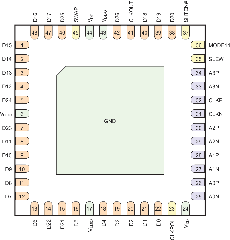
6 Pin Configuration and Functions
RGZ PACKAGE
(TOP VIEW)
SWAP Pin = Low or Floating
RGZ PACKAGE
(TOP VIEW)
SWAP Pin = High
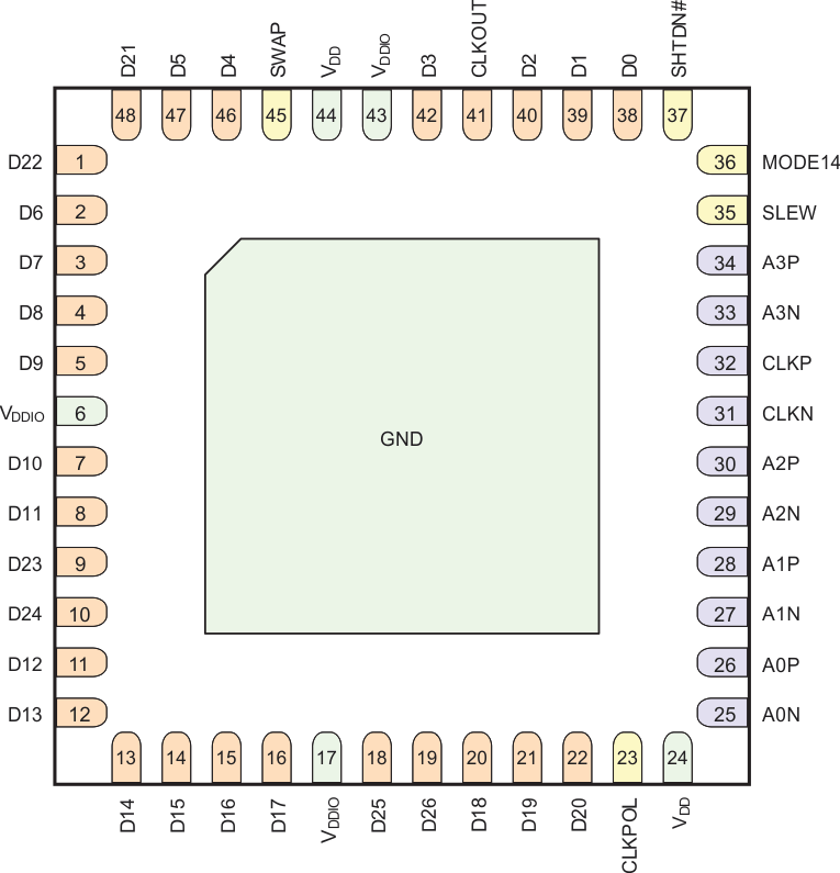
Pin Functions
| PIN | I/O | DESCRIPTION | |
|---|---|---|---|
| NAME | NO. | ||
| A0P, A0N | 26, 25 | LVDS Input | LVDS Data Lane 0 |
| A1P, A1N | 28, 27 | LVDS Data Lane 1 | |
| A2P, A2N | 30, 29 | LVDS Data Lane 2 | |
| A3P, A3N | 34, 33 | LVDS Data Lane 3 | |
| CLKP, CLKN | 32, 31 | LVDS Clock | |
| (SWAP = L / H) | CMOS Output | Data bus output | |
| D0 | 22 / 38 | ||
| D1 | 21 / 39 | ||
| D2 | 20 / 40 | ||
| D3 | 19 / 42 | ||
| D4 | 18 / 46 | ||
| D5 | 16 / 47 | ||
| D6 | 13 / 2 | ||
| D7 | 12 / 3 | ||
| D8 | 11 / 4 | ||
| D9 | 10 / 5 | ||
| D10 | 9 / 7 | ||
| D11 | 8 / 8 | ||
| D12 | 4 / 11 | ||
| D13 | 3 / 12 | ||
| D14 | 2 / 13 | ||
| D15 | 1 / 14 | ||
| D16 | 48 / 15 | ||
| D17 | 47 / 16 | ||
| D18 | 40 / 20 | ||
| D19 | 39 / 21 | ||
| D20 | 38 / 22 | ||
| D21 | 15 / 48 | ||
| D22 | 14 / 1 | ||
| D23 | 7 / 9 | ||
| D24 | 5 / 10 | ||
| D25 | 46 / 18 | ||
| D26 | 42 / 19 | ||
| CLKOUT | 41 | Clock output for the data bus | |
| SWAP | 45 | CMOS Input | Selects the CMOS output pinout, and also controls differential input termination. |
| Low – Default pinout, RID connected | |||
| Floating – Default pinout, RID disconnected (requires external termination) | |||
| High – Swapped pinout, RID connected | |||
| MODE14 | 36 | Sets the number of LVDS serial bits per lane per clock period. | |
| Low – 7 bits (see Figure 16) | |||
| High – 14 bits; only lanes A0 and A2 are used (see Figure 17) | |||
| CLKPOL | 23 | CLKOUT polarity | |
| Low – D[26:0] is valid during the CLKOUT falling edge | |||
| Floating – Reserved; do not use | |||
| High – D[26:0] is valid during the CLKOUT rising edge | |||
| SHTDN# | 37 | Shutdown Mode; Active-Low | |
| SLEW | 35 | Sets the CMOS output slew rate | |
| Low – Slowest rise/fall time | |||
| Floating – Medium rise/fall time | |||
| High – Fastest rise/fall time | |||
| VDD | 24, 44 | Power Supply | Main power supply; 3.3 V |
| VDDIO | 6, 17, 43 | Power supply for CMOS outputs; 1.8 V to 3.3 V | |
| GND | Thermal Pad | Reference Ground | |