ZHCSBQ4B September 2013 – September 2014 SN65LVDS822
PRODUCTION DATA.
- 1 特性
- 2 应用范围
- 3 说明
- 4 修订历史记录
- 5 说明(继续)
- 6 Pin Configuration and Functions
- 7 Specifications
- 8 Parameter Measurement Information
- 9 Detailed Description
- 10Application and Implementation
- 11Power Supply Recommendations
- 12Layout
- 13器件和文档支持
- 14机械封装和可订购信息
12 Layout
12.1 Layout Guidelines
Use 45 degree bends (chamfered corners), instead of right-angle (90°) bends. Right-angle bends increase the effective trace width, which changes the differential trace impedance creating large discontinuities. A 45o bends is seen as a smaller discontinuity.
Place passive components within the signal path, such as source-matching resistors or ac-coupling capacitors, next to each other. Routing as in case a) creates wider trace spacing than in b), the resulting discontinuity, however, is limited to a far narrower area.
When routing traces next to a via or between an array of vias, make sure that the via clearance section does not interrupt the path of the return current on the ground plane below.
Avoid metal layers and traces underneath or between the pads off the DisplayPort connectors for better impedance matching. Otherwise they will cause the differential impedance to drop below 75 Ω and fail the board during TDR testing.
Use solid power and ground planes for 100 Ω impedance control and minimum power noise.
For a multilayer PCB, it is recommended to keep one common GND layer underneath the device and connect all ground terminals directly to this plane. For 100 Ω differential impedance, use the smallest trace spacing possible, which is usually specified by the PCB vendor.
Keep the trace length as short as possible to minimize attenuation.
Place bulk capacitors (i.e. 10 μF) close to power sources, such as voltage regulators or where the power is supplied to the PCB.
12.2 Layout Example
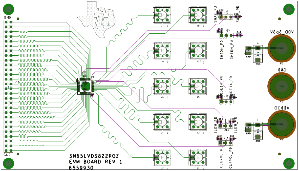 Figure 22. Layout Example
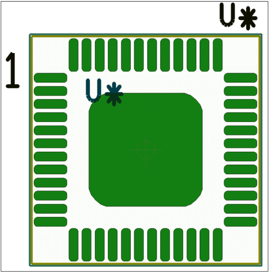 Figure 23. Footprint Example