ZHCSBQ4B September 2013 – September 2014 SN65LVDS822
PRODUCTION DATA.
- 1 特性
- 2 应用范围
- 3 说明
- 4 修订历史记录
- 5 说明(继续)
- 6 Pin Configuration and Functions
- 7 Specifications
- 8 Parameter Measurement Information
- 9 Detailed Description
- 10Application and Implementation
- 11Power Supply Recommendations
- 12Layout
- 13器件和文档支持
- 14机械封装和可订购信息
10 Application and Implementation
NOTE
Information in the following applications sections is not part of the TI component specification, and TI does not warrant its accuracy or completeness. TI’s customers are responsible for determining suitability of components for their purposes. Customers should validate and test their design implementation to confirm system functionality.
10.1 Application Information
10.1.1 Color Bit Mapping
The SN65LVDS822 is a simple deserializer that ignores bit representation in the LVDS stream. The CMOS output pin order was chosen so that if the color mapping within the LVDS stream matches the common VESA standard, the parallel output bus of red/green/blue fans out sequentially, which matches the order that many LCD panels require. Some LCD panels require a reversed order; for those, set pin “SWAP” high to reverse the output bus and simplify PCB routing. Figure 19 shows the application setup when SWAP is in different statuses.
Any color bit mapping is supported, by correctly connecting the output to the panel. However, bit “RSV” is ignored and unavailable for use.
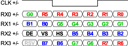 Figure 18. Common VESA Color Bit Mapping
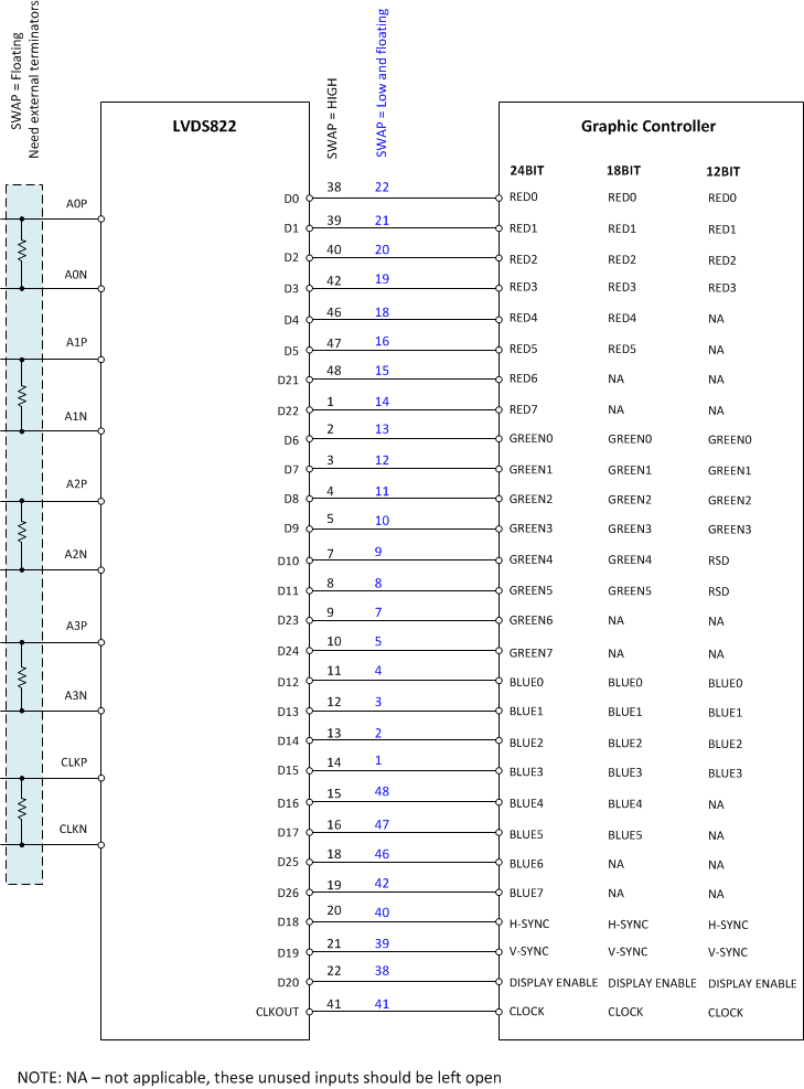 Figure 19. Pin Assignments With SWAP
10.2 Typical Application
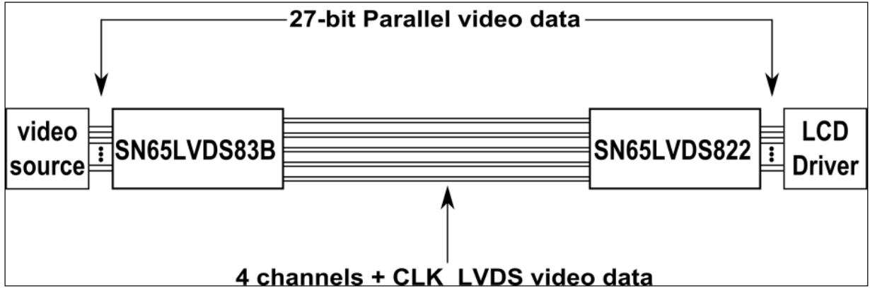 Figure 20. Typical Application
10.2.1 Design Requirements
| DESIGN PARAMETERS | VALUE |
|---|---|
| VDD Main Power Supply | 3 - 3.6 V |
| VDDIO Power Supply for CMOS Outputs | 1.65 - 3.6 V |
| Input LVDS Clock Frequency | 4 - 54 MHz |
| RID Differential Input Termination Resistance | 80 - 132 Ω |
| LVDS Input Channels | 2 or 4 |
| Output Load Capacitance | 1 pF |
10.2.2 Detailed Design Procedure
10.2.2.1 Power Supply
The implementation operates from the power provided by two banana jack connectors (P1 and P3) common ground. The VDD pin (P1) is connected to the main power supply to the SN65LVDS822 device and must be 3.3 V (±10%). The VDDIO pin (P3) is connected to the power supply of the SN65LVDS822 CMOS outputs and must be in the range of 1.8 to 3.3 V.
10.2.2.2 CMOS Output Bus Connector
Color Bit Mapping shows the CMOS output and bit mapping. Because some LCD panels require a reversed order, the SN65LVDS822 device is capable of reversing the output bus and simplifying PCB routing. When the pin is tied to high, the CMOS outputs are in normal order, otherwise the CMOS outputs are in reverse order.
10.2.2.3 Power-Up Sequence
The SN75LVDS822 does not require a specific power up sequence.
It is permitted to power up IOVCC while VCC remains powered down and connected to GND. The input level of the SHTDN during this time does not matter as only the input stage is powered up while all other device blocks are still powered down. It is also permitted to power up all 3.3V power domains while IOVCC is still powered down to GND. The device will not suffer damage. However, in this case, all the I/Os are detected as logic HIGH, regardless of their true input voltage level. Hence, connecting SHTDN to GND will still be interpreted as a logic HIGH; the LVDS output stage will turn on. The power consumption in this condition is significantly higher than standby mode, but still lower than normal mode. The user experience can be impacted by the way a system powers up and powers down an LCD screen. The following sequence is recommended:
Power up sequence (SN75LVDS83B SHTDN input initially low):
- Ramp up LCD power and SN65LVDS822 (maybe 0.5ms to 10ms) but keep backlight turned off.
- Wait for additional 0-200ms to ensure display noise won’t occur.
- Enable video source output; start sending black video data.
- Toggle LVDS83B shutdown to SHTDN = VIH.
- Toggle LVDS822 shutdown to SHTDN = VIH.
- Send > 1 ms of black video data; this allows the LVDS83B to be phase locked, and the display to show black data first.
- Start sending true image data.
- Enable backlight.
Power Down sequence (SN75LVDS83B SHTDN input initially high):
- Disable LCD backlight; wait for the minimum time specified in the LCD data sheet for the backlight to go low.
- Video source output data switch from active video data to black image data (all visible pixel turn black); drive this for > 2 frame times.
- Set SN75LVDS83B input SHTDN = GND; wait for 250 ns.
- Set SN75LVDS822 input SHTDN = GND; wait for 250 ns.
- Disable the video output of the video source.
- Remove power from the LCD panel for lowest system power.
10.2.3 Application Curve
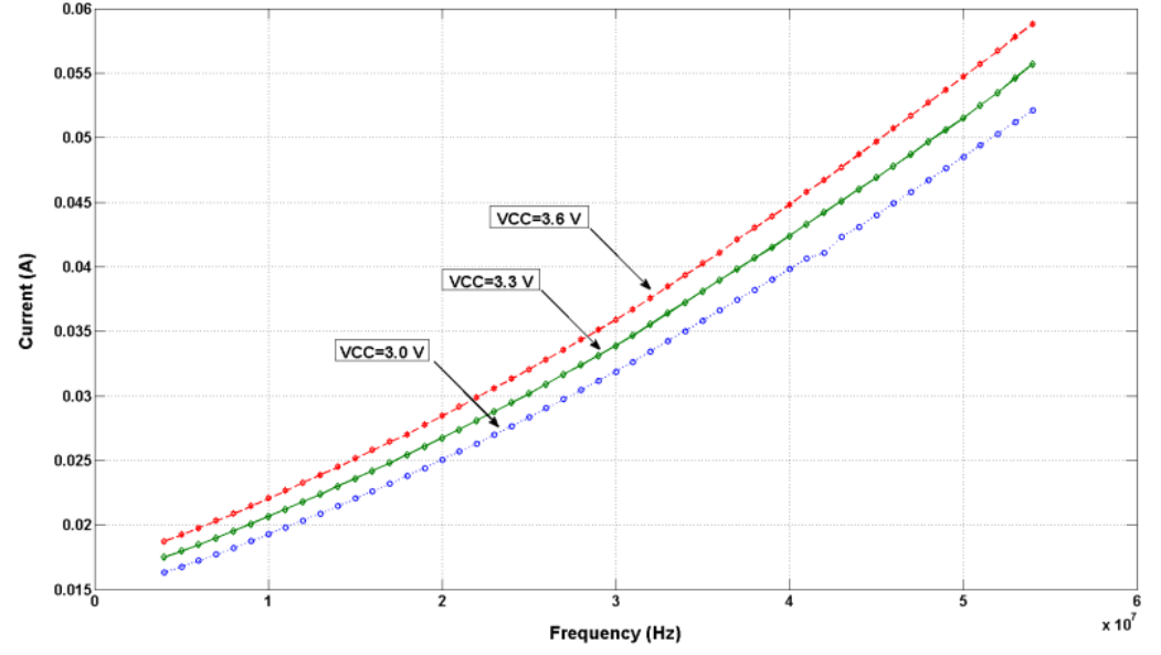 Figure 21. Total Current Consumption (VDD & VDDIO)