ZHCS603D November 2011 – April 2022 SN65HVDA100-Q1
PRODUCTION DATA
- 1 特性
- 2 应用
- 3 说明
- 4 说明(续)
- 5 Revision History
- 6 Pin Configuration and Functions
- 7 Specifications
- 8 Parameter Measurement Information
-
9 Detailed Description
- 9.1 Overview
- 9.2 Functional Block Diagram
- 9.3
Feature Description
- 9.3.1 LIN (Local Interconnect Network) Bus
- 9.3.2 TXD (Transmit Input / Output)
- 9.3.3 RXD (Receive Output)
- 9.3.4 VSUP (Supply Voltage)
- 9.3.5 GND (Ground)
- 9.3.6 EN (Enable Input)
- 9.3.7 NWake (High Voltage Wake Up Input)
- 9.3.8 INH (Inhibit Output)
- 9.3.9 TXD Dominant State Timeout
- 9.3.10 Thermal Shutdown
- 9.3.11 Bus Stuck Dominant System Fault: False Wake-Up Lockout
- 9.3.12 Undervoltage on VSUP
- 9.3.13 Unpowered Device Does Not Affect the LIN Bus
- 9.4 Device Functional Modes
- 10Application and Implementation
- 11Power Supply Recommendations
- 12Layout
- 13Device and Documentation Support
- 14Mechanical, Packaging, and Orderable Information
10.2.3 Application Curves
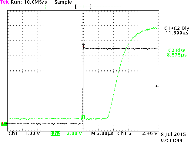
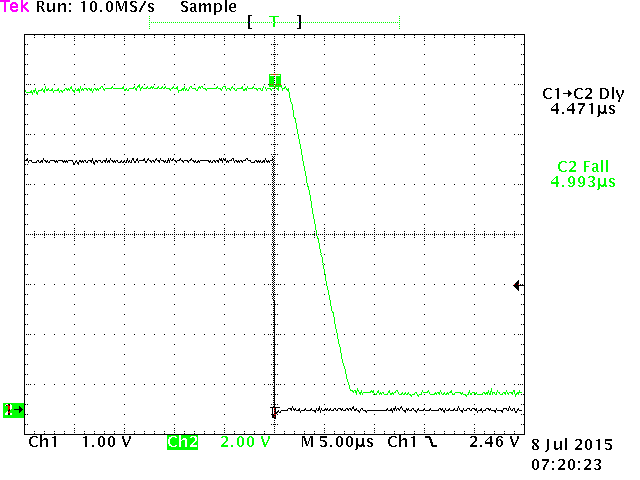
Figure 10-2 and Figure 10-3 show the propagation delay from the TXD pin to the LIN pin for both the recessive-to-dominant and dominant-to-recessive states under lightly loaded conditions.
 Figure 10-2 Dominant-to-Recessive Propagation Delay
 Figure 10-3 Recessive-to-Dominant Propagation Delay