ZHCSE43 July   2015 SN65HVD63

PRODUCTION DATA.  

  1. 特性
  2. 应用
  3. 说明
  4. 修订历史记录
  5. Device Comparison Table
  6. Pin Configuration and Functions
  7. Specifications
    1. 7.1 Absolute Maximum Ratings
    2. 7.2 ESD Ratings
    3. 7.3 Recommended Operating Conditions
    4. 7.4 Thermal Information
    5. 7.5 Electrical Characteristics
    6. 7.6 Switching Characteristics
    7. 7.7 Typical Characteristics
  8. Parameter Measurement Information
  9. Detailed Description
    1. 9.1 Overview
    2. 9.2 Functional Block Diagram
    3. 9.3 Feature Description
      1. 9.3.1 Coaxial Interface
      2. 9.3.2 Reference Input
      3. 9.3.3 RS-485 Direction Control
    4. 9.4 Device Functional Modes
  10. 10Application and Implementation
    1. 10.1 Application Information
      1. 10.1.1 Driver Amplitude Adjust
      2. 10.1.2 Direction Control
      3. 10.1.3 Direction Control Time Constant
      4. 10.1.4 Conversion Between dBm and Peak-to-Peak Voltage
    2. 10.2 Typical Application
      1. 10.2.1 Design Requirements
      2. 10.2.2 Detailed Design Procedure
      3. 10.2.3 Application Curve
  11. 11Power Supply Recommendations
  12. 12Layout
    1. 12.1 Layout Guidelines
    2. 12.2 Layout Example
  13. 13器件和文档支持
    1. 13.1 相关文档 
    2. 13.2 社区资源
    3. 13.3 商标
    4. 13.4 静电放电警告
    5. 13.5 Glossary
  14. 14机械、封装和可订购信息

封装选项

机械数据 (封装 | 引脚)
散热焊盘机械数据 (封装 | 引脚)
订购信息

8 Parameter Measurement Information

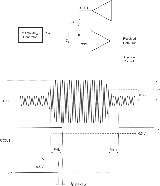
Signal generator rate is 115 kbps, 50% duty cycle. Rise and fall times are less than 6 ns, and nominal output levels are 0 V and 3 V. Coupling capacitor, CC, is 220 nF.
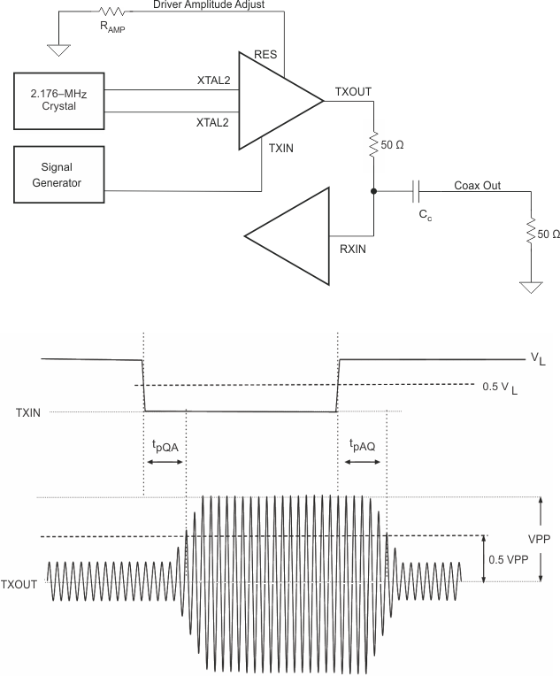
SN65HVD63 dvr_output_sllseo3.gif Figure 19. Measurement of Modem Driver
Output Voltage With 50-Ω Loads
SN65HVD63 rec_delay_sllseo3.gif Figure 20. Measurement of Modem Receiver Propagation Delays
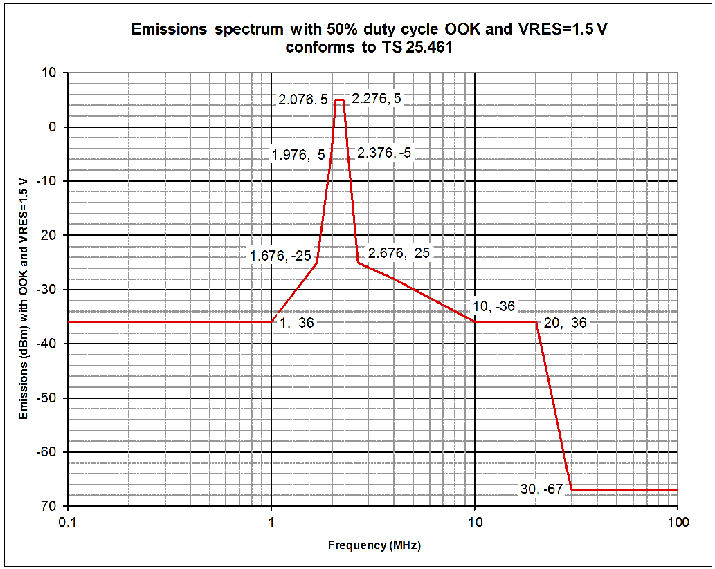
SN65HVD63 emissions_template_sllseo3.png Figure 21. AISG Emissions Template