ZHCSE43 July 2015 SN65HVD63
PRODUCTION DATA.
9 Detailed Description
9.1 Overview
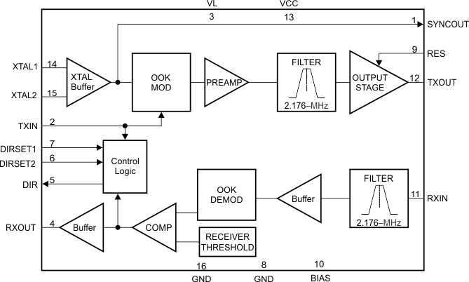
The SN65HVD63 transceiver modulates and demodulates signals between the logic (baseband) and a frequency suitable for long coaxial media. The SN65HVD63 device is an integrated AISG transceiver designed to meet the requirements of the upcoming Antenna Interface Standards Group v3.0 specification. The SN65HVD63 receiver integrates an active bandpass filter to enable demodulation of signals even in the presence of spurious frequency components. The filter has a 2.176-MHz center frequency. The transmitter supports adjustable output power levels from 0 dBm to 6 dBm delivered to the 50-Ω coax cable. The SN65HVD63 transmitter is compliant with the spectrum emission requirement provided by the AISG standard. A direction control output facilitates bus arbitration for an RS-485 interface. This device integrates an oscillator input for a crystal, and also accepts standard clock inputs to the oscillator.
9.2 Functional Block Diagram

9.3 Feature Description
9.3.1 Coaxial Interface
The SN65HVD63 transceiver enables the transfer of data between radio equipment by modulating baseband data to a carrier frequency of 2.176 MHz (per the AISG standard). The transmitter output amplitude can be configured from 0 dBm to 6 dBm in order to communicate over a variety of different links, and the output emissions spectrum is designed to be compliant to AISG limits. The receiver features an active bandpass filter circuit that helps to separate the carrier frequency data from other spurious frequency components.
9.3.2 Reference Input
The 2.176-MHz modulation frequency is derived from an input reference that is nominally 8.704 MHz. The input reference can come either from a crystal or from an oscillator circuit with a tolerance of up to 30 ppm.
9.3.3 RS-485 Direction Control
To facilitate bus arbitration of an RS-485 interface, the SN65HVD63 provides a direction control output that can be used to control the enable/disable controls of an RS-485 transceiver. The direction control output automatically toggles based on activity present on the coaxial input interface, and has an adjustable time constant (controlled by the DIRSET1 and DIRSET2 pins) in order to accommodate various signaling rates.
9.4 Device Functional Modes
If DIRSET1 and DIRSET2 are in a logic high state, the device will be in standby mode. While in standby mode, the receiver functions normally, detecting carrier frequency activity on the RXIN pin and setting the RXOUT state. The transmitter circuits are not active in standby mode, thus the TXOUT pin is idle regardless of the logic state of TXIN. The supply current in standby mode is significantly reduced, allowing power savings when the node is not transmitting.
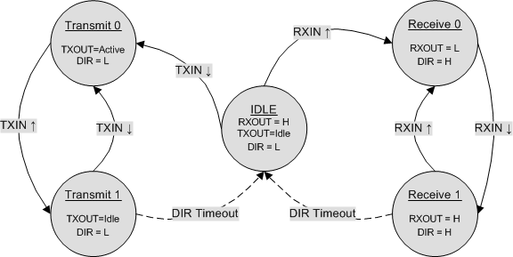
When not in standby mode, the default power-on state is idle. When in idle mode, RXOUT is high, and TXOUT is quiet. The device transitions to receive mode when a valid modulated signal is detected on the RXIN line or the device transitions to transmit mode when TXIN goes low. The device stays in either receive or transmit mode until DIR time-out (nominal 16 bit times) after the last activity on RXOUT or TXIN.
When in receive mode:
- RXOUT responds to all valid modulated signals on RXIN, whether from the local transmitter, a remote transmitter, or long noise burst.
- TXOUT responds to TXIN, generating 2.176-MHz signals on TXOUT when TXIN is low, and TXOUT is quiet when TXIN is high. (In normal operation, TXIN is expected to remain high when the device is in receive mode.)
- The device stays in receive mode until 16 bit times after the last rising edge on RXOUT, caused by valid modulated signal on the RXIN line.
When in transmit mode:
- RXOUT stays high, regardless of the input signal on RXIN.
- TXOUT responds to TXIN, generating 2.176-MHz signals on TXOUT when TXIN is low, and TXOUT is quiet when TXIN is high.
- The device stays in transmit mode until 16 bit times after TXIN goes high.
Table 1 shows the driver functions. Table 2 shows the receiver functions. Figure 22 shows the transitions between each state.
Table 1. Driver Function Table
| TXIN(1) | [DIRSET1, DIRSET2] | TXOUT | COMMENT |
|---|---|---|---|
| H | [L,L], [L,H] or [H,L] | < 1 mVPP at 2.176 MHz | Driver not active |
| L | VOPP at 2.176 MHz | Driver active | |
| X | [H,H] | < 1 mVPP at 2.176 MHz | Standby mode |
Table 2. Receiver and DIR Function Table
| RXIN(1) | RXOUT | DIR | COMMENT (see Figure 22) |
|---|---|---|---|
| IDLE mode (not transmitting or receiving) | |||
| < VIT at 2.176 MHz for longer than DIR time-out | H | L | No outgoing or incoming signal |
| RECEIVE mode (not already transmitting) | |||
| < VIT at 2.176 MHz for less than tDIR time-out | H | H | Incoming 1 bit, DIR stays HIGH for DIR time-out |
| > VIT at 2.176 MHz for longer than tnoise filter | L | H | Incoming 0 bit, DIR output is HIGH |
| TRANSMIT mode (not already receiving) | |||
| X | H | L | Outgoing message, DIR stays LOW for DIR time-out |
 Figure 22. State Transition Diagram