ZHCSE43 July 2015 SN65HVD63
PRODUCTION DATA.
10 Application and Implementation
NOTE
Information in the following applications sections is not part of the TI component specification, and TI does not warrant its accuracy or completeness. TI’s customers are responsible for determining suitability of components for their purposes. Customers should validate and test their design implementation to confirm system functionality.
10.1 Application Information
10.1.1 Driver Amplitude Adjust
The SN65HVD63 device can provide up to 2.5 V of peak-to-peak output signal at the TXOUT pin to compensate for potential loss within the external filter, cable, connections, and termination. External resistors are used to set the amplitude of the modulated driver output signal. Resistors connected across RES and BIAS set the output amplitude. The maximum peak-to-peak voltage at TXOUT is 2.5 V, corresponding to 6 dBm on the coaxial cable. The TXOUT voltage level can be adjusted by choice of resistors to set the voltage at the RES pin. according to the following equation:
The voltage at the RES pin should be from 0.7 V to 1.5 V. Connect RES directly to the BIAS (R1 = 0 Ω) for maximum output level of 2.5 VPP. This gives a minimum voltage level at TXOUT of 1.2 VPP, corresponding to about 0 dBm at the coaxial cable. A 1-μF capacitor should be connected between the BIAS pin and GND. To obtain a nominal power level of 3 dBm at the feeder cable as the AISG standard requires, use R1 = 4.1 kΩ and R2 = 10 kΩ that provide 1.78 VPP at TXOUT.
10.1.2 Direction Control
In many applications the mast-top modem that receives data from the base distributes the received data through an RS-485 network to several mast-top devices. When the mast-top modem receives the first logic 0 bit (active modulated signal) it takes control of the mast-top RS-485 network by asserting the direction control signal. The duration of the direction control assertion should be optimized to pass a complete message of length B bits at the known signaling rate (1/tBIT) before relinquishing control of the mast-top RS-485 network. For example, if the messages are 10 bits in length (B=10) and the signaling rate is 9600 bits per second (tBIT = 0.104 ms) then a positive pulse of duration 1.7 ms is sufficient (with margin to allow for network propagation delays) to enable the mast-top RS-485 drivers to distribute each received message. Figure 23 shows the assertion of direction control.
 Figure 23. Assertion of Direction Control
10.1.3 Direction Control Time Constant
The time constant for the direction control function can be set by the control mode pins, DIRSET1 and DIRSET2. These pins should be set to correspond to the desired data rate. With no external connections to the control mode pins, the internal time constant is set to the maximum value, corresponding to the minimum data rate.
10.1.4 Conversion Between dBm and Peak-to-Peak Voltage
Table 3 shows conversions between dBm and peak-to-peak voltage with a 50-Ω load, for various levels of interest including reference levels from the 3GPP TS 25.461 Technical Specification.
Table 3. Conversions Between dBM and Peak-to-Peak Voltage
| SIGNAL ON COAX | dBm | VPP |
|---|---|---|
| Maximum Driver ON Signal | 5 | 1.12 |
| Nominal Driver ON Signal | 3 | 0.89 |
| Minimum Driver ON Signal | 1 | 0.71 |
| AISG Maximum Receiver Threshold | –12 | 0.16 |
| Nominal Receiver Threshold | –15 | 0.11 |
| Minimum Receiver Threshold | –18 | 0.08 |
| Maximum Driver OFF Signal | –40 | 0.006 |
10.2 Typical Application
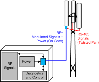
The AISG On-Off Keying (OOK) interface allows for command, control, and diagnostic information to be communicated between a base station and the corresponding tower-mounted antennae. Figure 24 shows a typical application.
 Figure 24. Typical AISG Application
10.2.1 Design Requirements
An AISG transceiver is used to convert between digital logic-level signals and RF signals. The AISG standard requires an RF carrier frequency of 2.176 MHz with 100-ppm accuracy. The output signal of the driver, when active, should be from 1 dBm to 5 dBm. The receiver must be designed such that the input threshold is from –18 dBm to –12 dBm.
10.2.2 Detailed Design Procedure
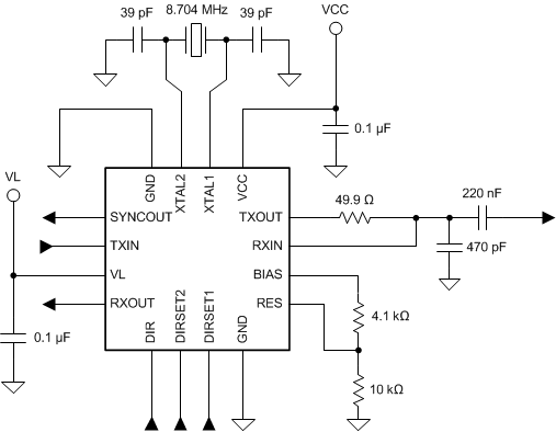
To ensure accuracy of the carrier frequency, an input reference frequency equal to four times the carrier (that is, 8.704 MHz) should be connected to the XTAL1 or XTAL2 inputs. This signal can come from a crystal (connected between XTAL1 and XTAL2) or from a PLL/clock generator circuit (connected to XTAL1 with XTAL2 grounded). The frequency accuracy must be within 100 ppm.
The driver output power level of the SN65HVD63 device can be adjusted through use of the RES pin. To align with AISG requirements, a nominal power level of 3 dBm should be configured by connecting a 4.1-kΩ resistor between RES and BIAS and a 10-kΩ resistor between RES and GND. Figure 25 shows an example schematic.
 Figure 25. SN65HVD63 Schematic
10.2.3 Application Curve
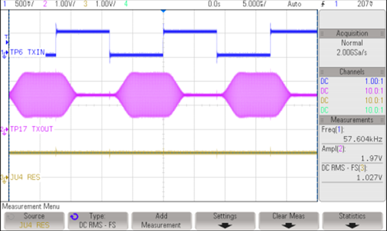
Figure 26 shows the application curve for the SN65HVD63 device.
