ZHCSE43 July   2015 SN65HVD63

PRODUCTION DATA.  

  1. 特性
  2. 应用
  3. 说明
  4. 修订历史记录
  5. Device Comparison Table
  6. Pin Configuration and Functions
  7. Specifications
    1. 7.1 Absolute Maximum Ratings
    2. 7.2 ESD Ratings
    3. 7.3 Recommended Operating Conditions
    4. 7.4 Thermal Information
    5. 7.5 Electrical Characteristics
    6. 7.6 Switching Characteristics
    7. 7.7 Typical Characteristics
  8. Parameter Measurement Information
  9. Detailed Description
    1. 9.1 Overview
    2. 9.2 Functional Block Diagram
    3. 9.3 Feature Description
      1. 9.3.1 Coaxial Interface
      2. 9.3.2 Reference Input
      3. 9.3.3 RS-485 Direction Control
    4. 9.4 Device Functional Modes
  10. 10Application and Implementation
    1. 10.1 Application Information
      1. 10.1.1 Driver Amplitude Adjust
      2. 10.1.2 Direction Control
      3. 10.1.3 Direction Control Time Constant
      4. 10.1.4 Conversion Between dBm and Peak-to-Peak Voltage
    2. 10.2 Typical Application
      1. 10.2.1 Design Requirements
      2. 10.2.2 Detailed Design Procedure
      3. 10.2.3 Application Curve
  11. 11Power Supply Recommendations
  12. 12Layout
    1. 12.1 Layout Guidelines
    2. 12.2 Layout Example
  13. 13器件和文档支持
    1. 13.1 相关文档 
    2. 13.2 社区资源
    3. 13.3 商标
    4. 13.4 静电放电警告
    5. 13.5 Glossary
  14. 14机械、封装和可订购信息

封装选项

机械数据 (封装 | 引脚)
散热焊盘机械数据 (封装 | 引脚)
订购信息

12 Layout

12.1 Layout Guidelines

Best practices for high-speed PCB design should be observed because the coax interface to the SN65HVD63 device operates at RF. The RF signaling traces should have a controlled characteristic impedance that is well-matched to the coaxial line. A continuous reference plane should be used to avoid impedance discontinuities. Power and ground distribution should be done through planes rather than traces to decrease series resistance and increase the effective decoupling capacitance on the power rails.

12.2 Layout Example
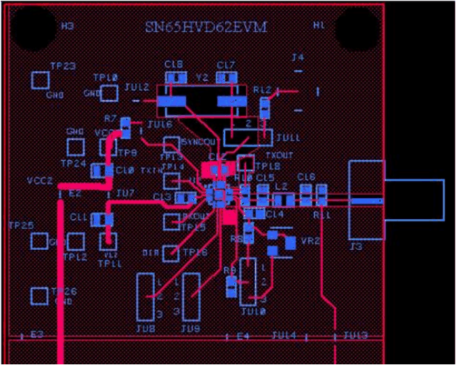
SN65HVD63 HVD63_Layout_Example_Top_SLLSEO3.gif Figure 27. SN65HVD63 Layout