ZHCSL25 April 2019 PCM1840
PRODUCTION DATA.
- 1 特性
- 2 应用
- 3 说明
- 4 修订历史记录
- 5 Pin Configuration and Functions
- 6 Specifications
-
7 Detailed Description
- 7.1 Overview
- 7.2 Functional Block Diagram
- 7.3
Feature Description
- 7.3.1 Hardware Control
- 7.3.2 Audio Serial Interfaces
- 7.3.3 Phase-Locked Loop (PLL) and Clock Generation
- 7.3.4 Input Channel Configurations
- 7.3.5 Reference Voltage
- 7.3.6 Microphone Bias
- 7.3.7
Signal-Chain Processing
- 7.3.7.1 Digital High-Pass Filter
- 7.3.7.2
Configurable Digital Decimation Filters
- 7.3.7.2.1
Linear Phase Filters
- 7.3.7.2.1.1 Sampling Rate: 8 kHz or 7.35 kHz
- 7.3.7.2.1.2 Sampling Rate: 16 kHz or 14.7 kHz
- 7.3.7.2.1.3 Sampling Rate: 24 kHz or 22.05 kHz
- 7.3.7.2.1.4 Sampling Rate: 32 kHz or 29.4 kHz
- 7.3.7.2.1.5 Sampling Rate: 48 kHz or 44.1 kHz
- 7.3.7.2.1.6 Sampling Rate: 96 kHz or 88.2 kHz
- 7.3.7.2.1.7 Sampling Rate: 192 kHz or 176.4 kHz
- 7.3.7.2.2 Low-Latency Filters
- 7.3.7.2.1
Linear Phase Filters
- 7.3.8 Dynamic Range Enhancer (DRE)
- 7.4 Device Functional Modes
- 8 Application and Implementation
- 9 Power Supply Recommendations
- 10Layout
- 11器件和文档支持
- 12机械、封装和可订购信息
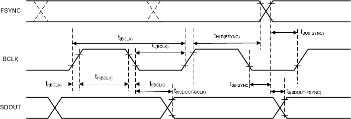
6.7 Switching Characteristics: TDM, I2S or LJ Interface
at TA = 25°C, IOVDD = 3.3 V or 1.8 V and 20-pF load on all outputs (unless otherwise noted); see Figure 3 for timing diagram| PARAMETER | TEST CONDITIONS | MIN | TYP | MAX | UNIT | |
|---|---|---|---|---|---|---|
| td(SDOUT-BCLK) | BCLK to SDOUT delay | 50% of BCLK to 50% of SDOUT | 18 | ns | ||
| td(SDOUT-FSYNC) | FSYNC to SDOUT delay in TDM or LJ mode (for MSB data with TX_OFFSET = 0) | 50% of FSYNC to 50% of SDOUT | 18 | ns | ||
| f(BCLK) | BCLK output clock frequency: master mode (1) | 24.576 | MHz | |||
| tH(BCLK) | BCLK high pulse duration: master mode | 14 | ns | |||
| tL(BCLK) | BCLK low pulse duration: master mode | 14 | ns | |||
| td(FSYNC) | BCLK to FSYNC delay: master mode | 50% of BCLK to 50% of FSYNC | 18 | ns | ||
| tr(BCLK) | BCLK rise time: master mode | 10% - 90% rise time | 8 | ns | ||
| tf(BCLK) | BCLK fall time: master mode | 90% - 10% fall time | 8 | ns | ||
(1) The BCLK output clock frequency must be lower than 18.5 MHz (to meet the timing specifications), if the SDOUT data line is latched on the opposite BCLK edge polarity than the edge used by the device to transmit SDOUT data.
 Figure 1. TDM, I2S, and LJ Interface Timing Diagram