ZHCSOX1 October   2020 OPA455

PRODUCTION DATA  

  1. 特性
  2. 应用
  3. 说明
  4. Revision History
  5. Pin Configuration and Functions
  6. Specifications
    1. 6.1 Absolute Maximum Ratings
    2. 6.2 ESD Ratings
    3. 6.3 Recommended Operating Conditions
    4. 6.4 Thermal Information
    5. 6.5 Electrical Characteristics
    6. 6.6 Typical Characteristics
  7. Detailed Description
    1. 7.1 Overview
    2. 7.2 Functional Block Diagram
    3. 7.3 Feature Description
      1. 7.3.1 Status Flag Pin
      2. 7.3.2 Thermal Protection
      3. 7.3.3 Current Limit
      4. 7.3.4 Enable and Disable
    4. 7.4 Device Functional Modes
  8. Application and Implementation
    1. 8.1 Application Information
    2. 8.2 Typical Applications
      1. 8.2.1 High DAC Gain Stage for Semiconductor Test Equipment
        1. 8.2.1.1 Design Requirements
        2. 8.2.1.2 Detailed Design Procedure
        3. 8.2.1.3 Application Curve
      2. 8.2.2 Improved Howland Current Pump for Bioimpedance Measurements in Multiparameter Patient Monitors
        1. 8.2.2.1 Design Requirements
        2. 8.2.2.2 Detailed Design Procedure
  9. Power Supply Recommendations
  10. 10Layout
    1. 10.1 Layout Guidelines
      1. 10.1.1 Thermally-Enhanced PowerPAD™ Package
      2. 10.1.2 PowerPAD™ Integrated Circuit Package Layout Guidelines
      3. 10.1.3 Pin Leakage
      4. 10.1.4 Thermal Protection
      5. 10.1.5 Power Dissipation
      6. 10.1.6 Heat Dissipation
    2. 10.2 Layout Example
  11. 11Device and Documentation Support
    1. 11.1 Device Support
      1. 11.1.1 Development Support
        1. 11.1.1.1 TINA-TI™ Simulation Software (Free Download)
        2. 11.1.1.2 TI Precision Designs
        3. 11.1.1.3 WEBENCH® Filter Designer
    2. 11.2 Documentation Support
      1. 11.2.1 Related Documentation
    3. 11.3 支持资源
    4. 11.4 Trademarks
    5. 11.5 静电放电警告
    6. 11.6 术语表
  12. 12Mechanical, Packaging, and Orderable Information

封装选项

机械数据 (封装 | 引脚)
散热焊盘机械数据 (封装 | 引脚)
订购信息

Typical Characteristics

at TA = 25°C, VS = ±75 V, and RL = 10 kΩ connected to GND, output enabled (unless otherwise noted)

Table 6-1 Table of Graphs
DESCRIPTION FIGURE
Offset Voltage Distribution at 25°C Figure 6-1
Offset Voltage Distribution at 85°C Figure 6-2
Offset Voltage Distribution at -40°C Figure 6-3
Offset Voltage Drift Distribution from -40°C to +85°C Figure 6-4
Offset Voltage vs Temperature Figure 6-5
Offset Voltage Warmup Figure 6-6
Offset Voltage vs Common-Mode Voltage (Low Vcm) Figure 6-7
Offset Voltage vs Common-Mode Voltage (High Vcm) Figure 6-8
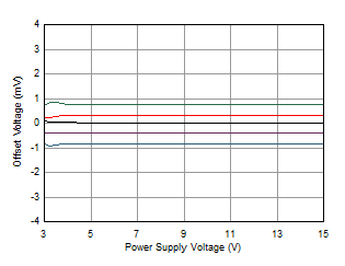
Offset Voltage vs Power Supply (Low Supply) Figure 6-9
Offset Voltage vs Power Supply (High Supply) Figure 6-10
Offset Voltage vs Output Voltage (Low Output) Figure 6-11
Offset Voltage vs Output Voltage (High Output) Figure 6-12
CMRR vs Temperature Figure 6-13
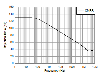
CMRR vs Frequency Figure 6-14
PSRR vs Temperature Figure 6-15
PSRR vs Frequency Figure 6-16
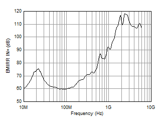
EMIRR vs Frequency Figure 6-17
No Phase Reversal Figure 6-18
Input Bias Current Production Distribution at 25℃ Figure 6-19
IB vs Temperature Figure 6-20
IB vs Common-Mode Voltage Figure 6-21
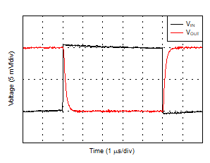
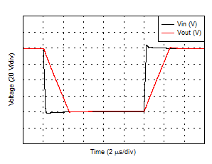
Enable Response Figure 6-22
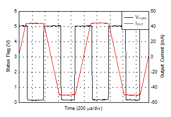
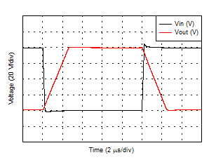
Current Limit Response Figure 6-23
Open-Loop Gain vs Temperature Figure 6-24
Open-Loop Gain vs Output Voltage Figure 6-25
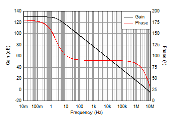
Open-Loop Gain and Phase vs Frequency Figure 6-26
Open-Loop Output Impedance vs Frequency Figure 6-27
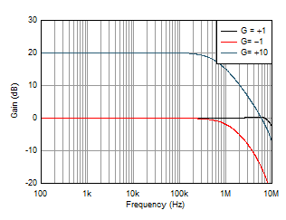
Closed-Loop Gain vs Frequency Figure 6-28
Maximum Output Voltage vs Frequency Figure 6-29
Positive Output Voltage vs Output Current Figure 6-30
Negative Output Voltage vs Output Current Figure 6-31
Short-Circuit Current vs Temperature Figure 6-32
Negative Overload Recovery Figure 6-33
Positive Overload Recovery Figure 6-34
Settling Time Figure 6-35
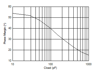
Phase Margin vs Capacitive Load Figure 6-36
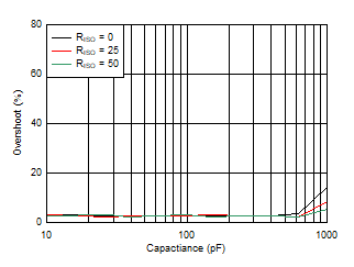
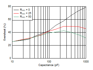
Small-Signal Overshoot vs Capacitive Load (G = –1) Figure 6-37
Small-Signal Overshoot vs Capacitive Load (G = +1) Figure 6-38
Small-Signal Step Response (G = –1) Figure 6-39
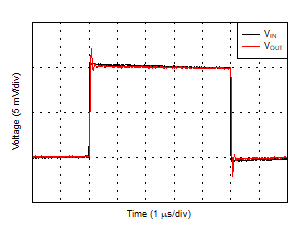
Small-Signal Step Response (G = +1) Figure 6-40
Large-Signal Step Response (G = –1) Figure 6-41
Large-Signal Step Response (G = +1) Figure 6-42
Slew Rate vs Output Step Size Figure 6-43
Slew Rate vs Supply Voltage (Inverting) Figure 6-44
Slew Rate vs Supply Voltage (Noninverting) Figure 6-45
THD+N Ratio vs Frequency (G = 10) Figure 6-46
THD+N Ratio vs Frequency (G = 20) Figure 6-47
THD+N Ratio vs Output Amplitude (G = 10) Figure 6-48
THD+N Ratio vs Output Amplitude (G = 20) Figure 6-49
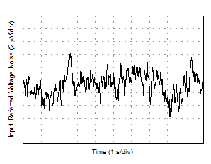
0.1-Hz to 10-Hz Noise Figure 6-50
Input Voltage Noise Spectral Density Figure 6-51
Current Noise Density Figure 6-52
Quiescent Current Production Distribution at 25℃ Figure 6-53
Quiescent Current vs Supply Voltage Figure 6-54
Quiescent Current vs Temperature Figure 6-55
Status Flag Voltage vs Temperature Figure 6-56
Quiescent Current vs Enable Voltage Figure 6-57
Enable Current vs Enable Voltage Figure 6-58
Status Flag Current vs Voltage Figure 6-59
 
Figure 6-1 Offset Voltage Distribution at 25°C
 
Figure 6-3 Offset Voltage Distribution at –40°C
 
Figure 6-5 Offset Voltage vs Temperature
 
Figure 6-7 Offset Voltage vs Common-Mode Voltage (Low VCM)
GUID-30FC4F31-6B10-4A05-9BCF-9E0D68CE49E4-low.gif
 
Figure 6-9 Offset Voltage vs Power Supply
(Low Supply)
 
Figure 6-11 Offset Voltage vs Output Voltage
(Low Output)
 
Figure 6-13 CMRR vs Temperature
 
Figure 6-15 PSRR vs Temperature
GUID-2083658B-FE81-41A5-AD97-73033389C327-low.gif
 
Figure 6-17 EMIRR vs Frequency
 
Figure 6-19 Input Bias Current Production Distribution at 25℃
 
Figure 6-21 IB vs Common-Mode Voltage
GUID-F0EBFDD2-2165-4D75-A311-CAE9583017BD-low.gif
 
Figure 6-23 Current Limit Response
 
Figure 6-25 Open-Loop Gain vs Output Voltage
 
Figure 6-27 Open-Loop Output Impedance vs Frequency
 
Figure 6-29 Maximum Output Voltage vs Frequency
 
Figure 6-31 Negative Output Voltage
vs Output Current
 
Figure 6-33 Negative Overload Recovery
 
Figure 6-35 Settling Time
GUID-913ED0E4-31BA-482D-92C8-FFCA3EA98E4E-low.gif
G = –1
Figure 6-37 Small-Signal Overshoot
vs Capacitive Load
GUID-3A46ADC2-5180-43CB-9AEE-8BFDC5C98171-low.gif
G = –1
Figure 6-39 Small-Signal Step Response
GUID-19A0150C-11DE-44F7-8403-72000CDE8F27-low.gif
G = –1
Figure 6-41 Large-Signal Step Response
 
Figure 6-43 Slew Rate vs Output Step Size
Figure 6-45 Slew Rate vs Supply Voltage (Noninverting)
G = 20
Figure 6-47 THD+N Ratio vs Frequency
G = 20
Figure 6-49 THD+N Ratio vs Output Amplitude
 
Figure 6-51 Input Voltage Noise Spectral Density
 
Figure 6-53 Quiescent Current Production Distribution at 25℃
 
Figure 6-55 Quiescent Current vs Temperature
 
Figure 6-57 Quiescent Current vs Enable Voltage
 
Figure 6-59 Status Flag Current vs Voltage
 
Figure 6-2 Offset Voltage Distribution at 85°C
 
Figure 6-4 Offset Voltage Drift Distribution
From –40°C to +85°C
 
Figure 6-6 Offset Voltage Warmup
 
Figure 6-8 Offset Voltage vs Common-Mode Voltage (High VCM)
 
Figure 6-10 Offset Voltage vs Power Supply
(High Supply)
 
Figure 6-12 Offset Voltage vs Output Voltage
(High Output)
GUID-1DC1B170-7F1D-41AA-A1B0-FCBC27BACF51-low.gif
 
Figure 6-14 CMRR vs Frequency
 
Figure 6-16 PSRR vs Frequency
 
Figure 6-18 No Phase Reversal
 
Figure 6-20 IB vs Temperature
 
 
Figure 6-22 Enable Response
 
Figure 6-24 Open-Loop Gain vs Temperature
GUID-14898377-F866-4FA0-8723-4F770312A6BF-low.gif
 
Figure 6-26 Open-Loop Gain and Phase vs Frequency
GUID-EB0281DB-4612-49F4-BEEF-AEA41C22E5A3-low.gif
 
Figure 6-28 Closed-Loop Gain vs Frequency
 
Figure 6-30 Positive Output Voltage
vs Output Current
 
Figure 6-32 Short-Circuit Current vs Temperature
 
Figure 6-34 Positive Overload Recovery
GUID-317C8BBE-F641-47A9-8911-08D2544F7C6C-low.gif
 
Figure 6-36 Phase Margin vs Capacitive Load
GUID-41EAC340-7339-4C63-B5E4-24D6C779332A-low.gif
G = +1
Figure 6-38 Small-Signal Overshoot
vs Capacitive Load
GUID-0277738E-F5DC-4012-B750-953E5981AB69-low.gif
G = +1
Figure 6-40 Small-Signal Step Response
GUID-A3D33885-D1C3-49D6-A376-DE64FCA4B110-low.gif
G = +1
Figure 6-42 Large-Signal Step Response
 
Figure 6-44 Slew Rate vs Supply Voltage (Inverting)
G = 10
Figure 6-46 THD+N Ratio vs Frequency
G = 10
Figure 6-48 THD+N Ratio vs Output Amplitude
GUID-111C445E-1F90-4967-BAE0-F46F6966DF3C-low.gif
 
Figure 6-50 0.1-Hz to 10-Hz Noise
 
Figure 6-52 Current Noise Density
 
Figure 6-54 Quiescent Current vs Supply Voltage
 
Figure 6-56 Status Flag Voltage vs Temperature
 
Figure 6-58 Enable Current vs Enable Voltage